What are the basics of synchronizing RS triggers circuit and synchronous D flip-flops?
1) Synchronous RS trigger
As long as the input signal changes, the basic RS trigger will immediately change the output state, which not only makes the anti-interference ability of the circuit worse, but also brings inconvenience to the synchronization work of multiple flip-flops. In practical applications, the state of the flip-flop is usually required to change at a certain time, that is, when the clock pulse arrives, the state is changed according to the input signal; when there is no clock signal, even if the input signal changes, the output state of the flip-flop is not affected. To this end, the clock input terminal CP and the corresponding input control circuit are added, and a digital chip such as a synchronous RS flip-flop is provided.
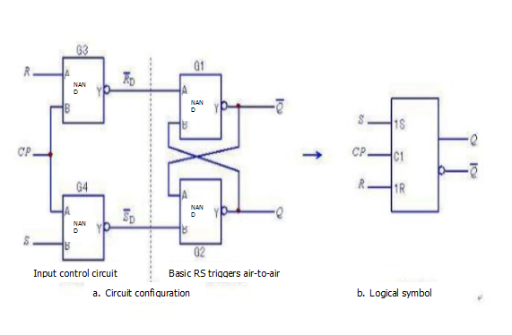
The circuit structure and logic symbols of the synchronous RS flip-flop are shown in Figure 1.

Figure 1 Synchronous RS Trigger
The NAND gates G1 and G2 constitute a basic RS flip-flop, and G3 and G4 constitute an input control circuit. The working principle is as follows:
a. During CP=0, NAND gates G3 and G4 are blocked, /RD=1, /SD=1. Therefore, no matter how the input signals R, S change, the output Q and /Q of the flip-flop are not affected, that is, the flip-flop state remains unchanged.
b. During CP=1, the NAND gates G3 and G4 are turned on, and the input signals R and S are inverted and applied to the basic RS flip-flop circuit composed of G1 and G2 to change the state of Q and /Q.
The function or state of the synchronous RS flip-flop can be described by a state transition table.
2) Synchronous D flip-flop
Synchronous RS Trigger after the R and S are both 1 and fail at the same time, the trigger status is uncertain, indicating that its function is still not perfect. The D trigger solves this problem and solves the problem that the trigger state is uncertain.
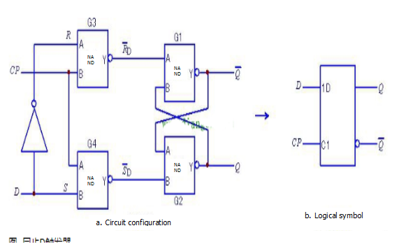
Since R or S are not equal to 1 at the same time, the trigger will not be unstable. The easiest way is to make S=/R. At this time, only S is used as the input (indicated by D), and obtained D trigger. It is still evolved from the RS trigger and is a special case of the RS flip-flop S=/R. Its circuit structure and logic symbols are shown in Figure 2.

Figure 2 Synchronous D flip-flop
The working principle is as follows:
a. During CP=0, NAND gates G3 and G4 are blocked, /RD=1, /SD=1. Therefore, no matter how the input signals R, S change, the output Q and /Q of the flip-flop are not affected, that is, the flip-flop state remains unchanged.
b. During CP=1, the NAND gates G3 and G4 are turned on, and the trigger output state changes with D, and three logic functions such as setting 0, setting 1, and holding are completed.
3) Double master-slave D-type flip-flop circuit maintenance example
There are too many forms of the trigger series circuit, it is unnecessary to fully understand it at once. Taking the dual master-slave D-type trigger CD4013 as an example, under the premise of not fully grasping the principle and internal circuit structure, can you quickly master the maintenance method according to the terminal function? The answer is yes.
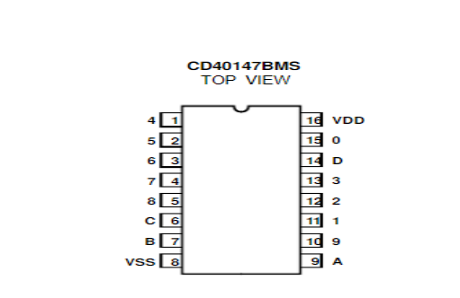
The core component of the control circuit is a dual D flip-flop, model CD4013, which contains two independent D flip-flops. Accepting a rising edge trigger signal from the R, S, or C terminals can cause the output state to toggle. Often used to form monostable, bistable, and unsteady circuits. As shown in Figure 3, it is a pin function diagram of the internal D flip-flop.

Figure 3 Pin function diagram of CD4014
We first master the two application modes of CD4013, and understand its circuit principle and action mode:
a) Data detection circuit. In the case where both the set terminal S and the reset terminal R are grounded, the data (0 or 1) of the D data terminal is transmitted to the output terminal Q under the action of the C-side clock pulse. There are only 0 or 1 data states on the D terminal, and the data at the D terminal is detected at the Q terminal during the rising pulse of the C terminal.
b) bistable circuit. In the case where both the data terminal D and the clock terminal C are grounded, a pulse high level is applied to the set terminal S, and the Q output terminal becomes a high potential (set); a pulse high potential is applied to the reset terminal R, Output Q goes low (reset).
According to this principle (or satisfying this detection condition), the CD4013 "transforms" into a normal R-S flip-flop, and applies a momentary high-level signal at the R and S terminals to complete the set, set, and hold function detection.
According to this principle (or satisfying this detection condition), a "0" or "1" signal can be artificially applied to the clock end to detect the data transmission state of the Q terminal and the D terminal, thereby accurately judging whether the chip is good or bad.
From the above, it is not necessary to study the complicated timing diagram of the digital circuit, and it is not necessary to control the transmission frequency and the specific transmission data. The circuit is only a high-low level signal processor, or only transmits a DC 5V and DC 0V signal circuit. The output is in these two states, and the input signal is also in these two states. It is fully usable with 0V and 5V as input detection signals to detect 5V and 0V variations at the output.
If you want to know more, our website has product specifications for the triggers, you can go to ALLICDATA ELECTRONICS LIMITED to get more information

