AMD Dual-Bridge RS880 Chipset Board Timing.
AMD mainboard timing characteristics.
The RTC circuit and the 25 MHz crystal are not referenced to the trigger.
The standby power supply S5 _ 3.3 V, the S5 1.1 V and the standby voltage good signal RSMRST # are normal and can be triggered.
The primary power supply sequence is the first memory power supply, the VDDA voltage, the CPU power supply, and finally the bridge power supply and the bus power supply. The timing analysis of MSI-7641 main board is as follows.
1. Plug in the ATX power supply, and the power supply gray line output VCC5_SB supplies the IO chip with 5 V power supply, as shown in Figure 1.

Fig.1 VCC5_SB supplies the IO chip with power supply.
2. The short switch needle produces the PWSW+trigger signal of the 5V-0V-5V jump, which is renamed PSIN, to the 76 pin of the IO chip after R548, as shown in figure 2.

Figure 2 IO chip triggers pin position.
3. IO chip sends out 3VSB_LAN_EN# low level signal from 48 pin to cut off Q69, pulls up to 5V high level via R648, and controls U38 chip to output 3VDUAL standby voltage, as shown in figure 3. At the same time,3VDUAL which provides standby power supply to IO chip and bridge .

Fig. 3 3VDUAL voltage generation circuit.
4.IO Chip 81 pin open leakage output RSMRST I0, after RN9 pull-up to 3.3V high level to G1 pin South Bridge chip SB850, indicating that the standby voltage is normal, as shown in figure 4.

Figure 4 RSMRST I0 pull-up circuit.
5.IO chip delay sends out the 3.3V-0V-3.3V jump PWRBTIN# signal from 77 pin (see figure 2) to the South bridge chip to request power on.
6. The South bridge chip outputs 3.3V persistent high level SLP_S5# and SLP_S3 # signals, as shown in figure 5.

Figure 5 SLP S5 # SLP S3 # output pin bits.
7. SLPS5#turns on the working output memory of U23 chip through the circuit conversion shown in Fig. 6. SLPS3#is sent to IO chip pin 78(see Fig. 2), indicating that power on is allowed.

Fig. 6 SLPS5#conversion circuit.
8. The IO chip outputs the low-level ATXPOSON#signal from pin 79 and sends it to the ATX power interface to pull down the green line, so that the power supply outputs each main power supply, as shown in Fig. 7.

Figure 7 ATX power interface.
9. After the clock chip gets 3.3V power, it starts to work and sends out clock signals to CPU, North Bridge chip, South Bridge chip, PCLE slot and network card chip.
10. The ATX power supply outputs 5V high-level ATXPWROK signal, one of which indicates normal power supply to the IO chip. The other is used to operate via the circuit shown in Fig. 8 and outputs 2.5V VDDA25 voltage to supply power to CPU.
11. Memory power supply and VDDA25 voltage are converted through the circuit shown in Figure 9 to obtain the low level signal of VCOREEN#.

Figure 8 VDD 25 generation circuit.
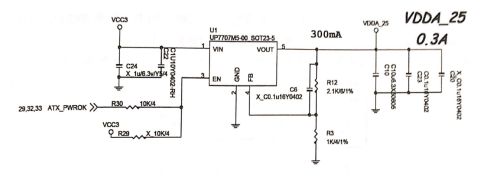
Figure 9 VCORE EN# generation circuit.
12.VCORE EN# controls Q15 cutoff. 12V through R107, R32 partial voltage to 1V VR EN high level (see figure 10), sent to the power management chip ISL6323 24 pin, turn on the chip to control the MOS tube step down to generate VCCP power supply to the CPU.
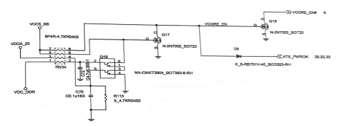
Fig. 10 VR EN generation circuit.
13. After the voltage of the VCCP is stable, the power management chip outputs the VCORE VLD (see FIG.10), and is pulled at a high level of 5V through the resistor R151, and the 84-pin to the 10-chip indicates that the VCORE is powered normally. 14.10 The chip issues 1.25 VREF NB and 12 VREF reference voltage, as shown in Figure 11.

Figure 11 10-chip output VREF reference voltage pin.
15.1.25 The VREF NB voltage controls the circuit operation shown in Figure 12 and Figure 13 to produce a + 1.8 V S0 supply and an NB1 2 V north bridge chip for power supply.

Figure 12 + 1.8 V S0 generation circuit.
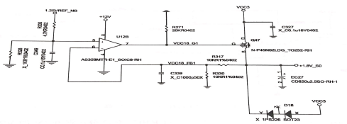
FIG. 13NB1 2V generation circuit.
16 1_2VREF reference voltage is sent to 3 pin of U18A through resistance R337, the voltage of 3 pin is higher than 2 pin voltage, and the output high level of 1 pin makes Q41 conduction on. VCC DDR gets VCCA 1VA power supply by Q41 step down. As shown in figure 14.1.2VREF, the reference voltage is sent to 3 pin of U40A through resistor R216, the voltage of 3 pin is higher than 2 pin voltage, and the high output level of 1 pin makes Q71 lead, VCC DDR step down to get 1.2 V power supply of VCC SB South Bridge chip, as shown in figure 15.
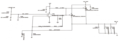
Fig. 14 VCCA 1V2 generation circuit.
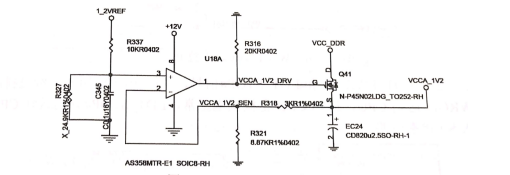
Fig. 15 VCC SB power supply generation circuit.
17. After the south bridge chip is supplied by VCC_ SB bridge, the internal clock module works and sends the clock signal to 10 chips, PCI slot and sound card chip. 18.NB1 2V north bridge chip power supply through the circuit shown in figure 16, and FP RST#,SLP S3 # phase and conversion to get 3.3V high level SYS PWRGD signal, to the south bridge chip PWR GOOD pin, indicating that the motherboard power supply is normal.
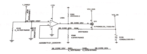
Fig. 16 SYS PWRGD generation circuit.
19. The south bridge chip sends the WD PWRGD signal to the high level of 1.8 V through the resistor R289 to inform the north bridge chip main board that the power supply is normal, as shown in Figure 17.

Figure 17WD PWRGD pull-up circuit.
20. The south bridge chip issues the LDT PWRGD and LDT STOP # signals. As shown in Figure 18, the LDT PWRGD is sent to the CPU through the size exclusion RN2 and the LDT PWRGD is sent to the CPU to inform the CPU main board that the power supply is normal, and the LDT STOP # is sent to the CPU and the north bridge chip to enter the S0 state circuit, respectively.

Fig.18 The south bridge chip of outputs the LTD signal.
21. The south bridge chip issues the SB PCI RST # signal to reset the I0 chip, and sends the SB PCIE RST # signal to reset the PCI-E. Slot.
22. The south bridge chip issues the LDT RST # signal, and the L8V high-level reset CPU and the north bridge chip are pulled over the RN2, as shown in FIG.19.
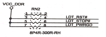
Figure 19 LDT RST # pull-up circuit.
If you want to know more, our website has product specifications for AMD Dual-Bridge RS880 Chipset Board, you can go to ALLICDATA ELECTRONICS LIMITED to get more information

