How to design the hardware of the Ethernet interface?
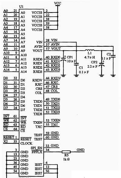
1.1 Interface design between W3150A + and FPGA
With the rapid development of semiconductor technology, the computing power, capacity, and reliability of FPGA (Field Programmable Gate Array) have greatly improved. It is becoming the new darling of digital circuits, digital signal processing and other fields with its advantages of highly flexible user field programming functions, repetitive rewriteable functions, and high reliability.
Considering cost, practicality and power consumption, the FPGA chip selected for this design is EPM570GT100C4 of Altera's MAXII series. The MAXII series device is a non-volatile CPLD, using a 0.18μm manufacturing process, and contains 240 to 2210 logic cells and 8Kbits of non-volatile memory, which can provide fast, stable, and more quantity than other CPLDs. Multiple I / O pins.
There are three ways of interface between W3150A + and microprocessor chip: direct bus interface mode, indirect bus interface mode and SPI mode. Among them, the direct bus interface mode is suitable for the transmission of large amounts of data; the SPI mode has fewer interface connections, which is suitable for the case where the data volume is not large and the transmission rate is relatively low; the data transmission performance in the indirect bus interface mode is between Between them. This system uses a direct bus interface mode to maximize the data transmission rate.
1.2 Interface design between the physical layer chip and W3150A +
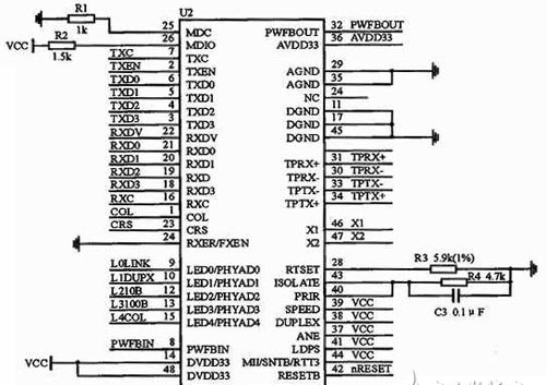
RTL8201BL is a single port physical layer transceiver, it has only one MII / SNI (Media Independent Interface / Serial Network Interface) interface. Can be used to implement all 10 / 100M Ethernet physical layer functions, including physical layer coding sublayer (PCS), physical layer media connection equipment (PMA), twisted pair physical media related sublayer (TP ~ PMD), 10Base-Tx Codec and twisted pair media access unit (TPMAU). The PECL interface can support the connection of an external 100Base-FX fiber optic transceiver. This chip is manufactured using advanced CMOS technology, which can meet the needs of low voltage and low power consumption.
RTL8201BL and W3150A + can be connected through a standard MII interface, where pins RX_CLK, RXDV, RXD [0: 3] and COL are used for data reception, and TX_CLK, TXE, TXD [0: 3] are used for data transmission. The specific circuit diagram is shown in the figure.

2 The realization process of data transmission
Through the controller to read and write access to the register, W3150A + can be connected to the network. The following describes the specific operation process.
It should be initialized first. Initial settings include basic settings, network information settings, port memory information settings, etc. After the settings are complete, data transmission can be performed. Data transmission can be carried out in TCP, UDP, IP_RAW and MAC_RAW modes, and the communication mode can be selected in the protocol type of port n mode register (Sn_MR). Among them, basic settings include mode register (MR), interrupt mask register (SIMR), retransmission time register (RTR), retransmission count register (RGR), etc .; setting network information includes setting gateway (GAR), setting source hardware Address (SHAR), set the subnet mask (SUBR), set the source IP address (SIPR), etc .; and set the port memory information is mainly to set the size of the send buffer and receive buffer allocation, specifically by setting The RMSR and TMSR registers are implemented.
Based on the FPGA chip EPM570GT100C4, this system can use the software Quartus II to develop logic control functions to realize the control of W3150A + The main ports are as follows:
nrst: reset input key, low level effective;
clk: clock input;
nwrst: reset output, can reset W3150A + and RTL8201;
nwr: write enable signal to W3150A +, low level effective;
nrd: read enable signal for W3150A +, active low;
ncs: W3150A + chip select signal, low level effective;
address: 15-bit address signal;
data: 8-bit data signal;
The communication design of this interface adopts UDP communication mode, and its communication flow chart is shown.
Port initialization is mainly to initialize the port, including setting the UDP mode, setting the port number, setting the OPEN command; through the value of the Sn_RX_RSR register can detect whether the data is received, if it is not zero, then enter the data receiving process; when receiving the process, first read The value of the Sn_RX_RSR register, that is, the number of received data bytes, then calculate the partial address and the actual physical address, and then read the data according to the physical address. In the process of reading data, if the physical address reaches the upper limit address set by the port, the data of the upper limit address is read first, then the physical address is changed to the base address, and then the remaining data is read from the base address. After reading all the data, you can add the value of Sn_RX_RR to the length of the read data, then write to sn_RX_BASE, and finally write the RECV command to the instruction register of port n.
send data? The implementation process of / send processing is to first read the value of the S_TX_FSR register so that the size of the send data space can be used to calculate the offset and actual physical address, and then write the data to be sent from the physical address. In the process of sending data, if the physical address has reached the upper limit address set by the port, the data is written to the upper limit address first, and then the physical address is changed to the base address, and then the data is continued to be written from the base address. After writing all the data, add the value of Sn_TX_WR to the length of the data sent, then write to Sn_TX_BASE, and finally write the SEND command to the instruction register of port n. The completion of sending can be determined after sending (SEND) command, by checking the value of Sn_CR to judge whether the data is all sent.
When the remote peer does not exist or the data transmission is abnormal, a timeout error will occur. This time, we can determine whether it is overtime by detecting Sn_IR (TIMEOUT bit). When all operations are completed, the window should be closed, that is, the Sn_CR register is set to CLOSE.
3 Conclusion
This article introduces the design of Ethernet interface and the process of data transmission. The method of this article can make the Ethernet interface operate normally, so it can lay the foundation for the subsequent development of virtual instruments. In fact, this method has been proved by many experiments: it fully meets the engineering needs.

If you want to know more, our website has product specifications for interface, you can go to ALLICDATA ELECTRONICS LIMITED to get more information

