What are the symbols represent in circuit diagram?
1.Signal.
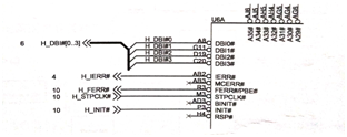
Fig. 1 illustrates the representation of the signal in the circuit diagram. A8, G11 and the like indicate the pin number of the CPU socket. DB10#, DBI1#, DBI2# are the data lines 0, 1, 2 of CPU socket. The signal is called HINIT# followed by the number, and 10 indicates that the signal is connected to page 10. The X in front of the H4 pin indicates that this signal is not used.

Fig.1 H_DBI#[0..3] Connection
The H_DBI# [0..3] shown in figure 1 is not actually connected together, but is simply drawn together for easy viewing. This signal expands into four separate signals after page 6, as shown in figure 2.

Fig.2 H_DBI#[0..3] Separation
2. The lines cross and connect.
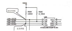
In fact, in the circuit diagram cross lines are not necessarily connected, the novice in the view of some wires are cross together, but others said this is interlinked, the other is not connected, always medicine is very chaotic. The cross well and the connected line have a solid point in the middle, and if the cross is not connected generally there is no solid point, as shown in Fig. 3.

Fig.3 Signal line cross connection
3. Common component symbols.
(1) Resistor.
Resistor symbols and parameters, shown in figure 4, represent resistor with a position number R4 with a resistance value of 10Ω.
(2)Network resistor.
The resistive symbol is shown in figure 5, with the RN45 indicating the resistive position number, the 8P4R indicating that there are eight pins with four independent resistors, and the 10KR indicating a resistor value of 10 kΩ per resistor.

Fig.4 Resistance symbol example Fig.5 An example of network resistor symbols
(3)Capacitors.
The symbols of the capacitance are shown in figs. 6 and 7. In Fig. 6, the EC45 indicates the capacitance position number, the capacitance has a one-pin grounding, the capacitance is the filter capacitance, the 1000U is the capacitance capacity, and the 6V3 indicates the capacitance voltage. In Fig. 7, C423 and C458 are capacitive position numbers, with capacitors in series in signal lines indicating that capacitors are coupling capacitors, CO.1U for capacitance capacity 0. 1 μ F, 16 for capacitance withstand voltage for 16 V, and 0402 for capacitor packaging.

Fig.6 Filter capacitor example Fig.7 Coupling capacitance example
(4)Inductance.
The inductance symbol is shown in figure 8.

(a)Patch inductance (b) Inductance coil
Fig.8 Inductance symbol
(5)Diode.
The diodes are divided into ordinary diodes, Schottky diodes, clamp diodes, and circuit symbols shown in figure 9.

(a)Ordinary diode (b)Schottky diode (c)Clamp diode
Fig.9 Diode symbol
(6)Voltage regulator.
The main board voltage regulator includes low-voltage differential linear voltage regulator and precision voltage regulator. The circuit symbol is shown in figure 10.

(a)Low-voltage differential linear (b)Precision voltage regulator
voltage regulator
Fig.10 Voltage regulator symbol
(7) Crystal oscillator.
The symbol of crystal oscillator circuit is shown in Fig. 11. X7 denotes the seventh crystal oscillator, and X-32.768K denotes the frequency of product vibration 32.768kHz.

Fig.11 Crystal oscillator symbol
(8) Triode.
The Triode symbol is shown in figure 12, the (a) arrow is outwardly represented as the NPN Triode, and the (b) arrow is shown inward as the PNP Triode.
(9) MOS tube.
In use, MOS transistors are commonly used in both N and P channels, and the circuit symbols are shown in figure 13.

(a)NPN triode(b)PNP triode (a)N channel MOS tube (b)P channel MOS tube
Fig.12 Triode symbol Fig.13 MOS tube symbol
LM358,LM324 and other devices are operational amplifiers, used in the main board to control the MOS tube voltage down to get the corresponding power supply, the circuit symbol is shown in figure 14.

Fig.14 Operational amplifier
(11) Gate circuits.
The common gate circuits in the circuit motherboard are non-gate, and gate or gate, and the circuit symbol is shown in figs. 15-17.

Fig.15 Non-gate symbol Fig.16 And gate symbols Fig.17 Or gate symbol
(12) Chip.
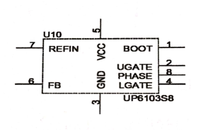
In addition to the basic electronic components, there are chips in the motherboard, such as memory power supply chip, power management chip and so on. These chips are usually square to lead the feet, and pin REFN in English, as shown in figure 18.

Fig.18 Chip symbol
4. Method of representation without mounting components.
The same model but different versions of the motherboard, components will not be the same, some components are not installed or multiple. In order to distinguish between installation and non-installation, the factory usually uses a symbol in the circuit diagram.

