What is the FPGA development process and how to use it after development?
l Development process
The FPGA design flow is the process of developing FPGA chips using EDA development software and programming tools. The development process of FPGA include the main steps of function definition/device selection, design input, function simulation, logic synthesis, place and route and implementation, and programming debugging.
1. Function definition/device selection: Before the start of the FPGA design project, there must be definition of system functions and division of modules. In addition, according to task requirements, such as the function and complexity of the system, the working speed and resources of the device itself. Trade-offs, costs, and the availability of connections, choose the right design and the right device type.
2. Design input: Design input refers to the use of hardware description language to express the designed system or circuit with code. The most common hardware description language is Verilog HDL.
3. Functional simulation: Functional simulation refers to the verification of the logic function of the circuit designed by the user before the logic synthesis. Before the simulation, it is necessary to set up the test platform and prepare the test stimulus. The simulation result will generate the report file and the output signal waveform, from which the signal changes of each node can be observed. If an error is found, return to the design modification logic design. Common simulation tools include Model Tech's ModelSim and Sysnopsys' VCS software.
4. Logic synthesis: The so-called synthesis is to transform the description of the higher level abstraction level into a lower level description. The integrated optimization optimizes the generated logical connections according to the target and requirements, and planarizes the hierarchical design for FPGA layout software. At the current level, comprehensive optimization refers to compiling design inputs into logically connected netlists composed of basic logic units such as AND gates, OR gates, NOT gates, RAMs, and flip-flops, rather than real gate-level circuits.
Real and specific gate-level circuits need to be generated by the FPGA manufacturer's place-and-route function based on the synthesized standard gate-level structure netlist. In order to be converted into a standard gate-level netlist, the HDL program must be written to match the style required by a particular synthesizer. Commonly used synthesis tools include Synplicity's Synplify/Synplify Pro software and comprehensive development tools from various FPGA vendors.
5, layout and implementation: layout can be understood as the use of tools to map the logic to the resources of the target device structure, determine the optimal layout of the logic, select the logic and the input and output function link routing channel to connect, and generate corresponding Files (such as configuration files and related reports); implementation is to configure the integrated generated logical netlist to a specific FPGA chip. Since only the FPGA chip manufacturer knows the chip structure best, the layout and wiring must choose the tools provided by the chip developer.
6, programming and debugging: the final step of the design is programming and debugging. Chip programming refers to the generation of the used data file (bitstream data file, Bitstream Generaon), loading the programming data into the FPGA chip; then the upper board test can be performed. Finally, the FPGA file (such as .bit file) is downloaded from the computer to the FPGA chip on the board.
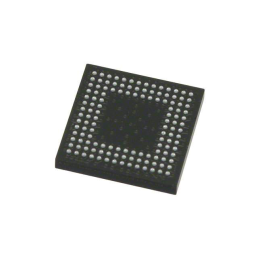
FPGA:LCMXO2-1200HC-4MG132I
l How to use FPGA
After the FPGA is developed, the verified load file is finally obtained. After outputting the load file, normal business processing and verification can be started (using the software loading method as an example to describe the whole process)
1. Logical loading;
2. After the board software loads the logic, it needs to reset the logic.


