CPU power supply principle.
The power management chip should control the MOS tube to depressurize to get the CPU power supply, whether it is the Intel or the AMD CPU power supply generation condition is the same, the power management chip gets the power supply VCC. After three conditions, VID signal and open signal EN, the control circuit works to produce VCORE, of course, the feedback circuit also needs to be normal. The main results are as follows:
(1) VCC is the power supply of main chip and driver chip, including VCC, PVCC, BOOT, BST stop and so on.
(2) EN is used to turn on the power management chip and control the timing of CPU power supply. It is controlled by foreign circuits, and the power supply management chip works at high normal times (usually more than IV). The EN pin names of common power management chips are EN, ENLL,DVD, VR_Enable, OUTEN, ENABLE, SHDN#, VCORE_EN, VRM_EN, etc.
(3) VID is a group of signals sent by CPU, which can be divided into parallel VID (PVID) and serial VID (SVID). VID (Voltage Identification, (voltage identification) is a voltage identification technology, VID signal is the signal from CPU, different CPU will have different VID combination, different CPU can generate different CPU voltage.
The principle of parallel VID (PVID) is to set 4 to 8 VID recognition pin on the CPU and form a set of VID recognition signals by preset high and low level values on these recognition pin . When the VID recognition pin is high level, it is the binary 1 state, when the VID recognition pin low level, it is the binary 0 state. According to the combination of 1 and 0, a basic set of machine language signals is formed. The well is transmitted from CPU to the power management chip in the CPU power supply circuit. According to the obtained VID signal, the power management chip adjusts the duty cycle of the output pulse signal, forcing the output DC voltage of the CPU power supply circuit to be consistent with the value represented by the preset VID.
The advantage of adopting VID technology is that it no longer uses hard jumper or DIP switch to adjust CPU voltage, and because of the programmable characteristics of VID technology, motherboard manufacturers can develop the function of adjusting CPU voltage by using BIOS. Some software can be used to realize the dynamic regulation of CPU voltage, which makes it convenient for some computer enthusiasts to pursue the function of over clocking.
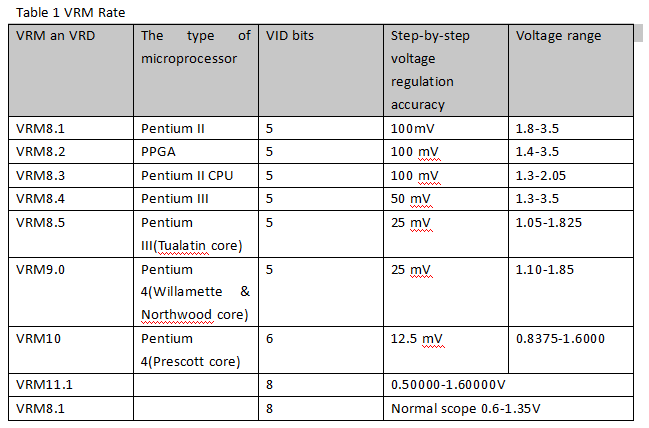
Intel has formulated the corresponding voltage regulator module (Volage Regulation model, VRM) design specification for each CPU produced by it at different times. Starting from the Prescott core microprocessor, the voltage regulation specification is named by VRD (Voltage regulation Down), and each version is named. The VID bits, voltage regulation accuracy, and voltage regulation you use vary from version to version of the power supply design specification. With the increase of VRM and VRD standards, the number of VID bits is gradually increasing, the precision of voltage regulation becomes smaller, and the range of voltage becomes smaller. Table 1.

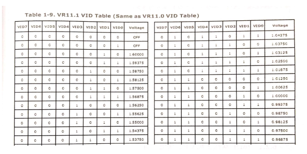
A partial screenshot of the VRD11.1 voltage regulator is shown in figure 1, where different combinations represent different voltages.

Fig. 1 partial screenshot of the VID11.1 voltage regulator table.
1. Parallel VID is simpler, that is, each set of VID corresponds to a variety of voltages. 6 bits correspond to 64 kinds of voltages in the sixth power of 2, and 8 bits correspond to 256 kinds of voltages. In the course of working, CPU gets the corresponding voltage for each set of VID output in the process of operation.
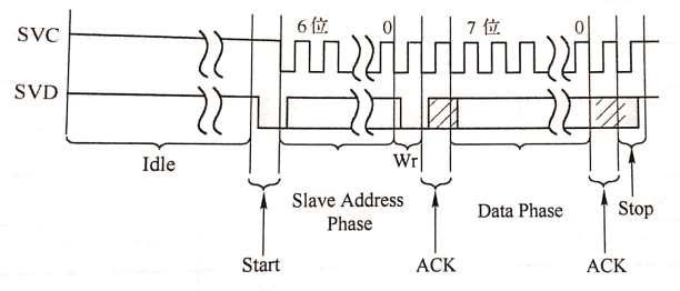
2. Serial VID is more complex, and SVC and SVD are simply clock signals and data signals.
As shown in figure 2, after the bus begins to work, the data transmitted by the data signal is recorded as an address during the first six clock cycles, and the data from the next clock cycle is recorded as read-write control, and then the data is judged to be valid or not. The data signal is followed by eight clock cycles. The address of the first six cycles is used to determine whether to control the CPU core voltage or the North Bridge chip voltage, and the 0 / 6 bit of the 8-bit data signal is used to control the voltage. Bit 7 is used to control PSI (energy-saving or low-power state control).The 0 / 6 bits of these 8-bit data signals are equivalent to the traditional 7-bit parallel VID positive and provide 128 voltage options. Using this mode, CPU can provide 0-6 bits of time-sharing data, controlling the core voltage and the North Bridge chip voltage, which is what we are doing now in N+1.

Figure 2 how SVID works.
Two different VID patterns can be said to be redefined for the needs of the development of CPU. For the PWM controller, it only changes the interface, and the principle part does not change much.
If you want to know more, our website has product specifications for CPU power supply principle, you can go to ALLICDATA ELECTRONICS LIMITED to get more information

