How to redefine FPGA ultra-low power ultra-small size?
Lattice's R&D engineers started the innovation of FPGA development process a few years ago, aiming to provide customers with hardware platforms with the above characteristics. In the end, Lattice became the industry's first low-power FPGA supplier to support a 28 nm fully depleted silicon-on-insulator (FD-SOI) process. This process was developed by Samsung and is similar to the bulk CMOS process used by most semiconductor chips today, but it has more significant advantages. It can significantly reduce device size and power consumption while greatly improving performance and stability.
In addition to supporting a new manufacturing platform, Lattice also relies on the industry experience of its low-power, small-size FPGA leading developers to achieve innovations at all levels of system design (from complete system solutions to FPGA architectures to circuits) , To further reduce power consumption, reduce the size of the FPGA, while improving system performance. The new manufacturing process and multiple levels of innovation gave birth to the Lattice Nexus™ FPGA development platform.
Lattice Nexus redefines low-power FPGA
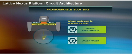
The FD-SOI process allows Lattice engineers to develop a new circuit design that takes full advantage of the inherent advantages of the process. One of its advantages is that FD-SOI supports programmable body bias (body bias), which is a block resistor located on the base of the transistor, allowing developers to dynamically adjust the transistor during operation. The programmable substrate bias invented by Lattice's R&D team can allow the device to run in high-performance mode or low-power mode according to the design's power consumption and thermal management needs. Only the software switch can control the operation mode. Developers can switch between high performance or low power consumption by programming the substrate bias voltage, which can optimize the power consumption/performance of the FPGA and better meet the application's power consumption and thermal management needs. This not only helps reduce the power consumption of battery-powered network edge devices, but also reduces the cost of electricity for industrial and data center applications. According to Lattice estimates, the power consumption of FPGAs based on the Nexus platform will be reduced by up to 75% compared with similar competitors.

Figure 1: Programmable substrate bias allows developers using Lattice FPGAs to closely control the leakage current of the circuit while fine-tuning the device to achieve low-power or high-performance modes.
Lattice Nexus accelerates AI processing performance
In order to support emerging technologies such as AI at the network edge, device developers need to make the system more intelligent. Their approach is to integrate more intelligent functions for the system, so that the device performs real-time data processing and analysis at the edge of the network. However, designers of AI face many challenges. AI inference algorithms require a lot of calculations, and also require a large storage module to store values locally for calculations. In the past, when developers of AI solutions needed a high-level DSP to implement algorithms, they often chose external resources, such as another processor in the system or the cloud. However, performing AI calculations off-chip will cause data delays, and in addition, sending customer data to the cloud will also cause data privacy problems and security risks.
With the Nexus FPGA technology platform, Lattice can solve the latency problem by integrating larger RAM and optimized DSP modules to store data locally and perform calculations. Nexus FPGAs have doubled the performance of previous Lattice FPGAs (while reducing power consumption by half), so developers can implement AI inference algorithms at the edge of the network. The potential applications of AI inference at the network edge include automatic industrial robots, ADAS systems, security cameras, and intelligent doorbells.
Lattice Nexus FPGA provides high stability
In general semiconductor devices, high-energy particles (such as cosmic rays and alpha particles) impinge on the transistor, and performance is impaired; this phenomenon is called soft error. Recovering from soft errors requires resetting the FPGA, which is obviously not suitable for critical applications that do not allow system interrupts for even a few milliseconds. In order to solve this problem, devices developed in bulk CMOS process usually use some functions to correct soft errors, such as on-chip soft error correction (SEC) and error code correction (ECC) modules. Lattice's FPGA based on the Nexus platform not only supports the above functions, but also has a very thin layer of oxide (thanks to the FD-SOI process) to protect the transistors in the FPGA and prevent high-energy particles from affecting the substrate. Therefore, the FPGA developed based on the Lattice Nexus technology platform can reduce the soft error rate by more than 100 times compared with similar FPGA products. As a result, the stability is greatly improved, which is ideal for any application, especially for some key applications in the automotive and industrial fields. The failure of its devices may cause significant personal injury and property damage.
Small size
The Lattice Nexus technology platform can also meet the continuous reduction in size of network edge devices. Many FPGA manufacturers are designing products for data analysis applications in the data center (cloud). Their architecture is large, and they are not suitable for small FPGAs with a small number of logic units. Lattice focuses on the development of small, low-power FPGAs, creating a compact FPGA architecture whose physical size is ten times smaller than competing FPGA products of similar logic density.
Lattice Nexus technology platform provides complete system solutions
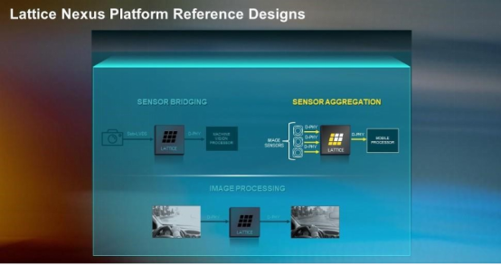
In addition to the innovations in the transistor structure on the Nexus technology platform, Lattice also studied higher-level abstract designs in the design process to understand how to help customers quickly and easily apply Nexus FPGAs in their application designs. Lattice has created or purchased and verified resources such as easy-to-use, intuitive design software, pre-designed soft IP modules, evaluation boards, kits, and complete reference designs to achieve the Lattice target market (communications, computing, industrial , Automotive, and consumer electronics) for various common applications, including sensor aggregation, sensor bridging, and image processing.
Figure 2: Lattice provides a complete reference design for the embedded vision market, allowing developers to quickly and easily enable new or existing product designs to support popular applications.
Let’s take a closer look at the sensor aggregation demo in Figure 2 and see how such demos can help customers quickly bring products to market. This demo is mainly used for embedded vision systems. It can obtain video data streams from up to four sources, combine them into one data stream, and then send it to a display or processor through high-speed MIPI D-PHY for subsequent processing. Potential applications for this demonstration include advanced driver assistance systems (ADAS). In this application, developers need to collect and aggregate data from multiple cameras and/or radar sensors, and then send it to the processor to make decisions in real time to ensure safety. Because there is no need to connect multiple sensors to the automotive application processor (AP), developers can simplify the routing on the system PCB and save valuable AP I/O ports, thereby reducing system cost and overall size.
In terms of software, FPGAs on the Lattice Nexus platform can be used with design software and Lattice's selected pre-verified IP libraries to implement various applications that the platform intends to support.
Launched the first FPGA based on Lattice Nexus: CrossLink-NX
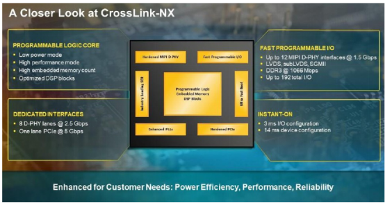
CrossLink-NX™ will be a huge opportunity as the first new product series developed on the Lattice Nexus technology platform. The new CrossLink-NX FPGA inherits the advantages of CrossLink series FPGAs in video signal bridging, splitting and aggregation applications, and also supports all video signal applications. Thanks to the Lattice Nexus development platform, the CrossLink-NX FPGA series has a higher storage logic ratio, a more optimized DSP, more logic units and faster I/O, and can use AI algorithms to process video data and run The speed is twice that of the previous FPGA. In addition, in industrial and automotive applications, CrossLink-NX is 10 times smaller than the previous generation, and the soft error rate is reduced by up to 100 times, greatly improving reliability. Finally, to further accelerate time to market, Lattice provides Diamond 2.0 FPGA development tools, proven IP modules, and application reference designs based on CrossLink-NX FPGAs.

Figure 3: CrossLink-NX series FPGAs are the first products developed based on the Lattice Nexus technology platform for AI and embedded vision applications.
in conclusion
Nowadays, while the fast-growing network edge equipment market requires higher performance and reliability, it is expected that the equipment has the characteristics of low power consumption and small size. Lattice has always focused on helping developers bring intelligent, low-power network edge devices to the market and serve various applications. With the launch of the Nexus platform, Lattice Semiconductor can quickly develop new FPGAs, and developers can accelerate product development to meet new market demands. The launch of the Lattice Nexus platform has redefined developers’ expectations for small, low-power FPGAs.
If you want to know more, our website has product specifications for FPGA, you can go to ALLICDATA ELECTRONICS LIMITED to get more information


