How to test the electromagnetic compatibility of the excitation switching power supply circuit?
In this paper, a flyback switching power supply is taken as an example to illustrate the generation and propagation mechanism of conduction common mode interference.
According to the idea of noise active node balance. It is verified by experiments that compared with the traditional design method, this method has stronger ability to suppress conducted electromagnetic interference (EMI) and can reduce the manufacturing cost and process complexity of the transformer. This method is equally applicable to other forms of switching power supplies with transformer topologies.
With the development of power semiconductor device technology, the high power-to-volume ratio and high efficiency of switching power supply make it widely used in modern military, industrial and commercial equipment, and with the increasing clock frequency, equipment The electromagnetic compatibility (EMC) problem has caused widespread concern. EMC design has become an indispensable part of the development and design of switching power supplies.
The suppression of conducted electromagnetic interference (EMI) noise must be considered early in product development. Normally, the installation of a power line filter is a necessary measure to suppress conducted EMI.
However, simply relying on a filter at the input of the power supply to suppress interference tends to result in increased inductance and increased capacitance of the components in the filter. The increase in inductance increases the volume; the increase in capacitance is limited by the leakage current safety standard. Other parts of the circuit can do the same work as filters if properly designed. In this paper, the phase-drying method of the noise active node of the transformer is proposed. This design method can not only reduce the volume of the power line filter, but also reduce the cost.
Common mode conducted interference of flyback switching power supplies
Conducted noise interference of an electronic device refers to electromagnetic interference that is transmitted to the public power grid environment through the power line in the form of noise current when the device is connected to the power supply network.
Conducted interference is divided into common mode interference and differential mode interference. The common mode interference current has the same phase on the neutral line and the phase line; the differential mode interference current has the opposite phase on the neutral line and the phase line. Differential mode interference has a small contribution to the overall conducted interference, and is mainly concentrated at the low frequency end of the noise spectrum, which is easier to suppress; common mode interference contributes a lot to the conducted interference, and is mainly in the intermediate frequency and high frequency bands of the noise spectrum.
The suppression of common mode conducted interference is a difficult and important task in the design of conductive EMC for electronic equipment.
There are some voltage drastic nodes in the circuit of the flyback switching power supply. Unlike other nodes in the circuit where the potential is relatively stable, the voltages at these nodes contain high-intensity high-frequency components .
These nodes whose voltage changes are very active are called noise active nodes. The noise active node is a common mode conducted interference source in the switching power supply circuit, which acts on the ground stray capacitance in the circuit to generate a common mode noise current ICM.
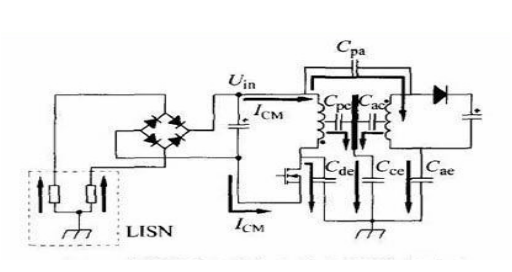
The stray capacitance of the circuit which has a great influence on EMI is: the parasitic capacitance Cde of the drain to ground of the power switch tube, the parasitic capacitance Cpa of the main side winding of the transformer to the secondary winding; the secondary side of the transformer is grounded The parasitic capacitance Cae, the parasitic capacitance Cpc, Cac of the main and secondary windings of the transformer and the parasitic capacitance Cce of the transformer core to the ground are distributed in the circuit as shown in Fig. 1.

Figure 1. Coupling path of common mode noise current in the circuit
The common mode current ICM in Figure 1 has three coupling paths in the circuit: from the noise source - the d pole of the power switch tube is coupled to ground through Cde; from the noise source through the Cpa to the transformer secondary circuit, and then through Cae is coupled to ground; the front and secondary windings of the transformer are coupled to the transformer core through Cpc and Cac, and then coupled to ground through Cce.
These three currents are the main factors that make up the common mode noise current (shown by the black arrow in Figure 1). The common mode current is recirculated through the ground of the input of the power line, which is measured by the LISN sampling.
Experimental part
The effectiveness of the transformer improved winding method on the conduction EMC performance of the switching power supply can be verified experimentally.
Experimental method
The frequency range is 0.15~30 MHz; the detection mode of the spectrum analyzer is quasi-peak detection; the measurement bandwidth is 9 kHz; the horizontal axis (frequency) of the spectrum is logarithmic; the unit of the noise signal is dBμV [5].

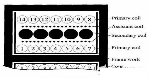
Figure 2. Transformer improved winding details
Experimental result
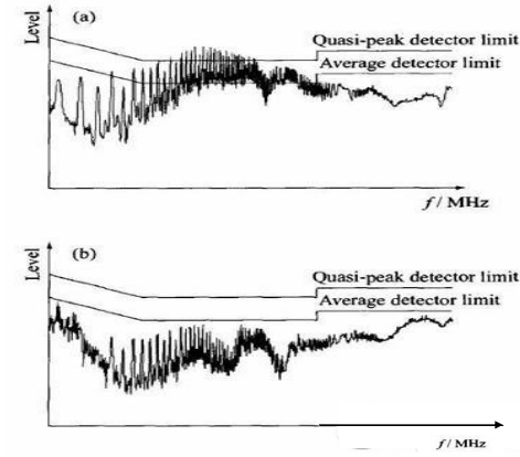
Figure 3 shows the comparison of conducted noise spectrum of experimental samples before and after transformer design improvement.

Figure 3. Noise spectrum before and after transformer design improvement
The upper and lower parallel fold lines in Figure 3 are the quasi-peak detection limit and the average detection limit of the b-level requirements of the CISPR22 standard promulgated by the International Special Committee on Radio Interference (CISPR); and the curve is the conducted noise spectrum of the switching power supply.
It can be seen from the experimental results that the new method has better suppression of common mode noise current than the conventional method, especially in the frequency range of 1 to 5 MHz. In the lower frequency band, the conducted interference on the power line is mainly caused by the differential mode current; in the middle and high frequency bands, the common mode current plays a major role. The method proposed in this paper has strong suppression of common mode current, and the experiment and theory are consistent. In the frequency band above 10 MHz, the EMC performance is mainly determined by other parasitic parameters in the circuit, and has little relationship with the transformer.
Conclusion
The noisy active node in the switching power supply circuit is a common mode noise source in the circuit. To reduce the level of conducted interference of the switching power supply, it is actually to reduce the common mode current intensity and increase the ground impedance of the noise source. In a traditional isolated EMC design, the isolation layer is connected to a node with stable potential in the circuit (eg, the negative pole of the transformer's front stage) more effectively than the direct connection to ground to suppress EMI interference.
The active nodes of the noise in the switching power supply circuit are usually in pairs. The phase between these pairs of nodes is opposite. With this feature, the phase equilibrium winding of the active node is more effective for EMI suppression than the traditional isolated design. Since there is no need to add an isolation metal layer, the volume and cost of the transformer can be effectively reduced or reduced.
If you want to know more, our website has product specifications for switching power supply, you can go to ALLICDATA ELECTRONICS LIMITED to get more information

