The demand for artificial intelligence to promote the FPGA market, can this innovation solve application bottlenecks?
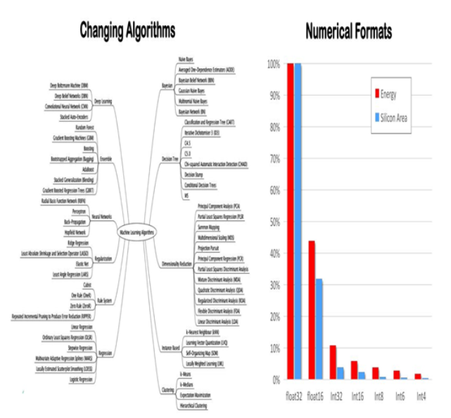
AI's algorithms are evolving, and the requirements for numerical precision are more diverse. Efficient computing, efficient and rich storage caching, and efficient and large-bandwidth data delivery capabilities are the main challenges faced by AI/ML hardware solutions. System developers use FPGA fabrics to optimize power, performance, and flexibility, and break through the bottleneck in the efficiency of the processing unitincluding computational engines, memory hierarchies, and data movement.

Figure: Different algorithms and accuracy requirements present challenges for processing
As far as AI applications are concerned, different scenarios have different requirements for FPGAs. Usually, the application in cloud computing mainly requires the acceleration ability of FPGA in AI/ML and high-bandwidth data, while on end side, it needs to have high flexibility and ASIC performance. Although FPGA has been widely used in the field of AI, whether it satisfies the requirements of these two aspects is still a topic worth exploring.
Refactoring FPGA architecture
Throughout the evolution history of FPGA products (including the generation of devices), each major iteration is a design methodology innovation. From this perspective, Achronix's recently released Speedster7t is optimized for the above two application scenarios. Can be seen as a methodological innovation. During the development of Speedster7t, Achronix's engineering team completely reimagined the entire FPGA architecture to balance on-chip processing, interconnects, and external input/output interfaces to maximize data-intensive application throughput. These scenarios can be found in edge-based and server-based AI/ML applications, network processing and storage.
Specifically, compared to current FPGAs, The Speedster7t innovation is the design of a ML-oriented processor (MLP) and a high-bandwidth two-dimensional network-on-a-chip (NOC) that can span and vertically span the FPGA logic array, both of which preserve the flexibility of the FPGA. The performance of the ASIC is also achieved.
MLP unit that does not occupy FPGA wiring
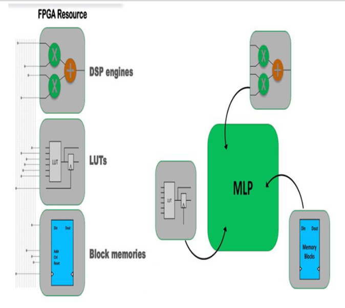
This on-chip MLP is a highly configurable, computationally intensive unit module that supports 4 to 24 bit integer point formats and efficient floating point modes, including support for TensorFlow's 16-bit format. The MLP can implement more complex algorithms through computational and cache-level chains without the need to use FPGA wiring resources.

Figure: Using MLP (right) in FPGA is more suitable for AI/ML processing than DSP (left)
Two-dimensional on-chip network - NOC
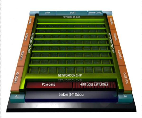
NOC is another important innovation in the FPGA routing architecture. This design focuses on the high bandwidth communication required between the on-chip processing engines of the FPGA. Speedster7t on-chip resources include eight GDDR6 controllers, 72 industry SerDes (1 to 112 Gbps), hardware 400G Ethernet MAC with forward error correction (FEC) (4x100G or 8x50G configuration), and hardware PCI Express Gen5 control (each controller has 8 or 16 channels).
These NOC and FPGA functions are connected by a network access point NAP, and each horizontal row and vertical column intersection has NAP (primary NAP and secondary NAP). Each row/column in the NoC can provide 512 Gbps of data traffic for each direction at the same time, and its link runs in both directions, and the maximum device bandwidth can reach 20 Tbps.

Indeed, the NOC method solves the problem of massive data transmission of on-chip resources such as GDDR6 and 400G Ethernet MAC. The Speedster7t is the only FPGA in the market that supports GDDR6 memory. It supports GDDR6 accumulation bandwidth of 4 Tbps and provides equivalent storage bandwidth with HBM-based FPGAs at a small cost. Compared to HBM, GDDR6 only needs half the cost to meet the high storage level and bandwidth requirements, and HBM is a solidified block, GDDR6 is more flexible, users can choose different capacity and bandwidth.
NOC also solves the problem that the running speed of traditional FPGA can not meet the requirements of any 400G Ethernet bus width. The bus size of 400G Ethernet is up to 1024bit, and the highest frequency required is 724MHz, which cannot be realized in traditional FPGA,. The NOC can support up to 750 MHz by eliminating the delay associated with FPGA routing in traditional designs, which satisfies data transfer between MLP and embedded memory modules, 400G Ethernet MAC, and high-speed SerDes.
If you want to know more, our website has product specifications for memory, you can go to ALLICDATA ELECTRONICS LIMITED to get more information.

