What are the advantages of analog switches for special applications?
As the demand for feature-rich handsets has grown stronger, analog switches with special application performance have continued to be favored by the final design. This will not only reduce the cost of materials (BOM), but also help improve design performance and meet time-to-market requirements. This article will guide system designers through several practical use cases to reduce pop noise, detect chargers.

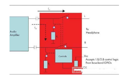
Impact noise caused by inrush currents is still a daunting challenge for designers, especially when the end user initiates a switch between music and call functions. As long as the end user turns on the music feature, this annoying noise can give an unpleasant experience. As shown in Figure 1, when the audio amplifier is operating, the on/off surge current through the AC coupling capacitor is the culprit of the impact noise, and the audio common mode voltage will rise sharply.
There are a variety of solutions available on the market today. One of them is to add an additional amplifier to give the audio output a "0V" offset, thereby minimizing the size of the ac coupling capacitor immediately before the earphone. Because most headphone amplifiers are integrated into a baseband processor or power management unit (PMU), adding this amplifier not only increases material costs but also increases power consumption.
Figure 1 shows another method that adds an independent charging path to the audio signal path to allow the AC coupling capacitor to be fully charged before being switched to the headphone or main path. This can be controlled by the baseband processor's general purpose I/O, allowing the audio amplifiers and switches to power up first, and the main channel switch is now off. The common mode voltage of the audio output will start to rise from 0 to VCC/2. After a period of time (referenced to 10ms), both ends of the coupling capacitor are charged to the equipotential, and then the main channel is turned on and there is no inrush current at all. Because, at this time, the voltage difference between the two poles of the capacitor is 0V.
This switch is ideal for mobile phones and MP3/MP4 players that are shared by headphones and USB data cables with a single USB connector (D+/D-pin). Low total harmonic distortion (THD) is very important for audio channels. In addition, since the switch is placed after the AC coupling capacitor, a large reverse signal swing at low THD must be handled. The ultra-low turn-off capacitor of this switch allows high-speed USB signals to be "wired" connected via the device. The lower parasitic capacitance is also the key to the compliance test of the Hi-Speed USB 2.0 standard.

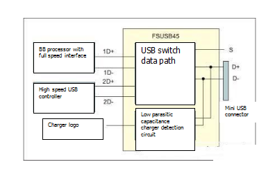
With the current market trend shifting to a single USB charger/data port, the special application USB switch has become a common configuration in handset design with charger detection. Figure 2 is an example of such a switch application.
Based on two main reasons, a low on capacitance switch is required in this design. First, since the baseband processor and the Hi-Speed USB controller output share the same D+/D- pins on the connector side, when the phone enters Hi-Speed USB 2.0 mode (such as music download or flash function), the baseband USB1.1/ must be lowered. The output capacitance of the 2.0 full speed controller. Any additional capacitance on the D+/D- line will damage the eye opening of the Hi-Speed USB signal. Secondly, in the high-speed USB mode, the extra traces on the D+/D- line must be cut off to effectively avoid signal reflection caused by the fast rising/falling edge of the 480Mbps USB signal.
Since a single USB port is used for both the charger and the data function, the charger detection function has become very popular in the current design. The conventional approach is to feed the D+/D- lines to the internal A/D converter to determine if the D+/D- lines are shorted. As mentioned earlier, the main limitation of this scheme is that the high input capacitance of the GPIO port of the baseband processor will add additional capacitive reactance on the data line. This new capacitive reactance will result in an effective triggering of the signal at high data rates. Adverse effects, which are part of the USB 2.0 compliance test (eg 480 Mbps for USB 2.0 signals). Of course, another disadvantage of this approach is that it also takes up resources of the system A/D converter.
In these applications, a USB switch with an ultra-low internal capacitance detection circuit is required to achieve charger isolation and isolation of the full-speed USB controller output capacitor. At the same time, the USB channel select pin (S-pin in Figure 2) used to determine which USB channel to use as the output must recognize the 1.8 V and 3 V logic inputs (Note: 1.8 V and 3 V in the baseband processor GPIO output are quite common).
The traditional switch select pin accepts input “high” (Vih) levels of up to 2.0 V (TTL logic), which can cause severe leakage currents when the switching power supply (VCC) is taken directly from the battery. The ability to recognize 1.8 V input logic levels also eliminates the need for external level shifting devices, allowing designers to further reduce material costs. For example, Fairchild's FSUSB45 and other ICs have ultra-low on-capacitance (7pF) and small size (1.4×1.8 mm), as well as charger detection and 1.8 V control logic recognition, which can well meet USB data path switches design needs.
If you want to know more, our website has product specifications for analog switches, you can go to ALLICDATA ELECTRONICS LIMITED to get more information

