What are the benefits of using FPGAs with on-chip high-speed networking?
Simplify team collaborative design
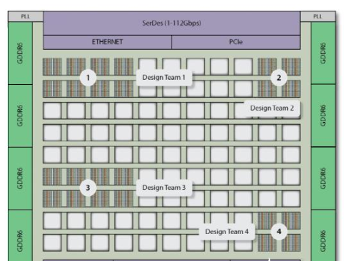
Team-based collaborative FPGA design is not a new concept, but the underlying architecture and wiring depend on other parts of the FPGA, making it very challenging to implement this simple concept. Once a team has completed part of the design, another team that designs other parts of the device will often encounter challenges when trying to access resources on the other end of the device, because the wiring needs to be done in the completed part of the design. Similarly, changes to the area or size of some FPGAs that have been designed and routed may have a knock-on effect on all other FPGA design modules.
Using Speedster7t NoC, design modules can be mapped to any part of the FPGA, and resource allocation can be changed without affecting the timing, layout or routing of other FPGA modules. Because all NAPs in the device support unlimited access to NoC for communication by each design module, it makes team-based design possible. Therefore, if a certain part of a design increases in scale, as long as there are enough FPGA resources available, the data flow will be automatically managed by the NoC, so that the designer does not have to worry about whether the timing is met, and other team members The possible follow-up effects of other parts of the design.

Figure 1: Multiple design teams working on the same FPGA
Speed up design through independent interface and logic verification
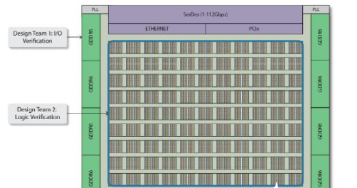
Another unique feature of Speedster7t NoC is to allow designers to configure and verify I/O connections independently of user logic. For example, one design team can verify the PCIe to GDDR6 interface, while another design team can independently verify the internal logic functions. This independent operation can be realized because the peripheral part of NoC is connected with PCIe, GDDR6, DDR4 and FCU without consuming any FPGA resources. These connections can be tested without using any HDL code, so that the interface and logic can be independently verified at the same time. This function eliminates the dependency between verification steps and achieves a faster overall verification speed than traditional FPGA architecture.

Figure 2: Independent I/O and logic verification
Use Packet Mode to simplify 400 Gbps Ethernet applications
The challenge in implementing a high-speed 400 Gbps Ethernet data path in an FPGA is to find a bus width that can meet the performance requirements of the FPGA. For 400G Ethernet, the only viable option for full-bandwidth operation is a 1,024-bit bus running at 724 MHz, or a 2,048-bit bus running at 642 MHz. Such a wide bus is difficult to route because they consume a lot of logic resources in the FPGA architecture, and even the most advanced FPGA will have timing closure challenges under such speed requirements.
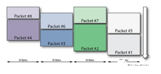
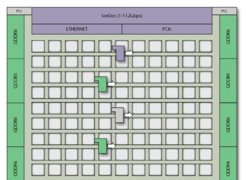
However, in the Speedster7t architecture, designers can use a new processing mode called packet mode, in which the incoming Ethernet stream is rearranged into four narrower 32-byte packets, or four independent 256-bit bus running at 506 MHz. The advantages of this mode include: when the data packet ends, the waste of bytes is reduced, and the data can be transmitted in parallel, instead of having to wait until the first data packet is completed before starting the second data packet transmission. The Speedster7t FPGA architecture is designed to enable the grouping mode by connecting the Ethernet MAC directly to a specific NoC column, and then using a user-instantiated NAP to connect from the NoC column to the logic array. Using the NoC column, data can be sent to any position in the FPGA fabric along the column for further processing. Using the ACE design tool to configure the packet mode can greatly simplify user design and improve efficiency when processing 400 Gbps Ethernet data streams.

Figure 3: Data bus rearrangement in packet mode

Figure 4: 400 Gbps Ethernet using packet mode
If you want to know more, our website has product specifications for FPGA, you can go to ALLICDATA ELECTRONICS LIMITED to get more information

