What is the working principle of the reset circuit of the Intel H55 chipset motherboard
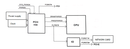
The reset circuit for the Intel single-bridge H55 chipset motherboard is shown in figure 1.

Figure 1 Intel single bridge H55 chipset motherboard reset circuit.
1. Short switch, the main board circuit began to work, through the supply circuit step-down to generate internal power supply, bridge power supply, bus power supply and CPU power supply voltage.
2. After the CPU power supply is stabilized, the power management chip outputs a high-level VR_RDY signal. The conversion of the circuit to the SYS_ PWROK bridge indicates that the CPU power supply is normal.
3. After the output voltage of ATX is stable, the ATX _ PWROK signal is delayed outputted to the 1O chip, and the high-level PWROK signal is output to the bridge through the internal conversion of the 1O chip, indicating that the power supply of the ATX power supply is normal.
4. After the mainboard power supply is normal, turn on the clock circuit to work, output the clock signal to the bridge.
5. The bridge power supply, the clock signal is normal, after receiving two PG signals, sends out the high level DRAMPWRGD signal to the CPU, to indicate the memory power is normal.
6. The bridge re-outputs the PROCPWRGD signal to the CPU, to indicate full board power supply is normal.
7. The bridge sends out a reset signal for the PLTRST# platform to reset the IO chip and the CPU.
8. The bridge finally issues the PCIRST# reset PCI slot.
9. After receiving the reset signal from the bridge, the IO chip generates the PCIRST2# reset PCI_E slot through the internal logic circuit, and the PCIRST1# reset the Nic chip.
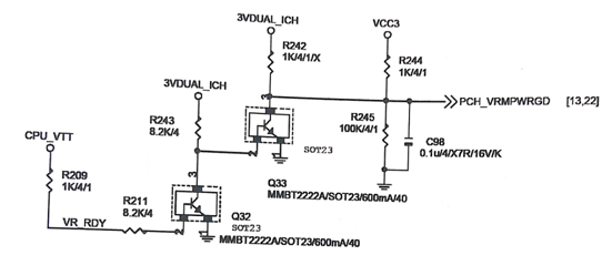
The SYS_ PWROK signal generation circuit is shown in fig. 2. After the power management chip is stabilized, the output high-level VR RdY signal is pulled up through R209 and sent to the B pole of Q32 through R221, making Q32 on and Q33 cut-off. The PCH VRMPWRGD is pulled to 3.267V high through the R244 and R245 partial voltages, and the SYS_PWROK pin sent to the bridge indicates that the CPU is powered properly.
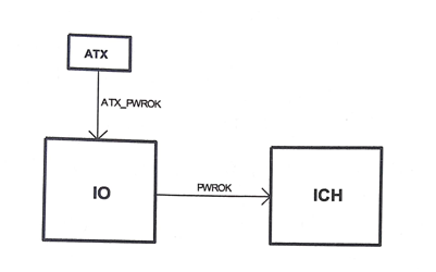
The principle of PWROK signal generation is shown in figure 3. ATX power output high-level ATX PWROK signal to the IO chip, after the internal logic conversion of the IO chip, output PWROK high-level 3.3V signal to the South Bridge chip to indicate that the power supply is normal. The common Huabang W83627 series IO chip outputs the PWROK signal from 71 pins to the South Bridge chip, and the Lianyang Series IO chip outputs the PWROK signal from 32 feet or 78 feet to the South Bridge chip.

Fig.2 SYS_PWROK signal generation circuit.

Fig.3 PWROK signal generation circuit.

