AMD Motherboard bus Power supply Analysis
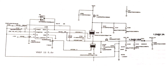
AMD chipset motherboard bus power supply from the North Bridge chip powered VCC_NB or South Bridge chip powered VCC_SB conversion, controlled by the ISL6545 chip to generate bus power supply, the working principle is shown in figure 1.

1. The + 12V voltage supplies 5-pin power to the chip via resistor R3181 and 1-pin power via the D4 Schottky diode BAT54.
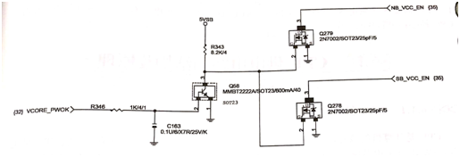
2. When the CPU power supply is normal, the VCORE_PWOK high level is output, and the SB_VCC_EN high level is generated through the circuit (see figure 2), which is sent to the chip 7 feet to open the chip to work.
3. The chip controls Q429 and Q430 from 2-pin and 4-pin output drive signals. The VCC3 step-down is supplied to 1.2V via L29, EC39 and EC33 output VCC_SB south bridge chip. After FB15 and EC25, it is renamed VCC12_HT to power the bus.

Figure 2 VCORE_PWOK conversion circuit.
In fig. 2, a high-level VCORE_PWROK power supply good signal sent out by the power management chip is sent to the B pole of the Q58 via a resistor R346 so that Q58 is switched on, Q279 and Q278 are cut off to obtain the high-level signal output of the NB_VCC_EN and SB_VCC_EN.
This article is from Allicdata Electronics Limited. Reprinted need to indicate the source.

