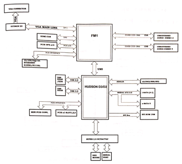
AMD single bridge A55 chipset motherboard architecture.
The AMD single bridge A55 chipset motherboard architecture is shown in figure 1.

Figure 1 AMD single bridge A55 chipset motherboard architecture diagram.
The management and support functions of the AMDA55 single bridge chipset motherboard are as follows.
①AMD motherboard switch to a single-bridge architecture from 9 series onwards, with A55 chip and AMD FM1CPU. used for the first generation single-bridge motherboard
② FM1 is the next generation of AMD to integrate the GPU display core and the CPU core into a single chip called APU.
③FM1 outputs video signals that support VGA analog signals, HDMI HD multimedia interfaces, and PCI-E X16 standalone video card slots.
④FMI CPU also integrates memory controllers to manage memory to support up to 1866MHz memory. 4FMI internal integrated network control module manages the 100MH Nic chip.
⑤The bridge is referred to as the connection between the FCH, and the APU using the UMI bus.
⑥FCH Management USB 2.0 Interface, USB 3.0 Interface, Sound Card Chip, SATA hard disk Interface, E-SATA external hard disk Interface, PCL-E XI slot, MINI PCI-E slot, and SPI BIOS.
⑦FCH manages the 10 chip through the LPC bus.
This article is from Allicdata Electronics Limited. Reprinted need to indicate the source.

