How the Intel H55 chipset motherboard works?
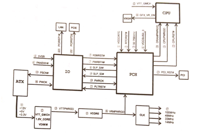
The Intel H55 chipset motherboard works as shown in figure 1.

Figure 1 schematic diagram of the Intel H55 chipset motherboard.
The Intel H55 chipset motherboard works as follows.
①VCCRTC powers the internal real-time clock circuit of the bridge.
② RTCRST# provides reset to the internal real-time clock circuit of the bridge.
③Crystal oscillator provides the bridge with 3.768Hz frequency.
④5VSB supplies IO chips with hold power, and VCCSUS3 _ 3 provides standby power to the bridge.
⑤IO chip sends a RSMRST# letter to the bridge, indicating that the motherboard standby power supply is good.
⑥The tap switch generates a PANSWH# trigger signal to be sent to the 1O chip.
⑦After internal conversion, the @ IO chip outputs the PWRBTN# signal to power up the bridge request.
⑧Bridge outputs a continuously high-level SLP S4 # message to the IO chip and turns on memory power.
⑨Bridge re-outputs a continuously high-level SLP_S3# signal to the IO chip to indicate that power is allowed.
⑩The IO chip outputs a continuously low-level PSONH-to-ATX power supply after internal conversion.
11. After the power supply green cable is pulled down, the main power supply such as + 12V, + 5V, + 33V is output to complete the power up.
12. Through the power supply circuit step down, get the memory power supply, bridge power supply, bus power supply.
13. The bus power supply outputs the VTTPWRGD signal through the circuit conversion to the EN pin of the power management chip that supplies the CPU with the power supply.
14. CPU gets the bus power, outputs the GFX_ VR_EN signal and turns on the video card.
15. The power management chip begins to work, and the control circuit depresses the voltage to get the VCORE to power the CPU.
16. The power management chip outputs the VRMPWRGD signal. All the way to the bridge indicates that the CPU power supply is normal, all the way to the clock chip.
17. The clock chip starts to work, outputs 10MHz, 48MHz, 33MHz, 14MHz and other clock signals to the bridge, and then sends the clock signals to each device.
18. ATX Power delay sends a PWOK signal to the 1O chip.
19. The 10 chip outputs the PWROK signal to the bridge through internal conversion, indicating that the power supply is normal.
20. The bridge sends a DRAMPWRGD signal to the CPU, to indicate that the memory is powered properly.
21. The bridge sends out a CPUPWRGD signal to the CPU to indicate that the motherboard is powered properly.
22. Bridge sends out PLIRST# signal reset 10 chip and CPU. The IO chip sends out PCRSTI# and PCIRST2# signals and resets the Nic chip and the PCIL_E slot.
23. The bridge sends out a PCI_RST# signal and resets the PCI slot.
This article is from Allicdata Electronics Limited. Reprinted need to indicate the source.

