How to explain the working principle of buffer network?
By analyzing the working process of the PFC main switch Q to illustrate the working principle of this lossless absorption buffer network.
1) When Q is turned on, because the current in inductor L2 cannot change suddenly, and the voltages in C2 and C1 cannot change suddenly, the current in Q increases from zero and rises slowly. The current iD4 through D4 gradually decreases. Q achieves zero current turn-on, with less conduction loss.
2) When the current iD4 decreases to zero, D4 enters the reverse recovery state, and the current iL2 = iL1 + irD4 through the inductor L2. The rate of change of D4 reverse current irD4 is controlled by the inductor L2, and the reverse recovery loss is reduced.
3) The current in the main inductor L2 increases slowly, and the voltage uQ on Q decreases. The capacitor C2 is discharged through D2, C1, L2, and Q, and the voltage uC2 on C2 drops.
4) When uC2 drops to zero, the energy in C2 turns to C1 and L2 completely. The current saturation in L2 does not change, uQ drops to zero, and Q completes the zero current turn-on process.
5) Q remains in the on state, the same as the switch state of the ordinary PFC circuit.
6) When Q is turned off, the current iL2 in L2 flows to C2 through D1, and C2 starts to charge from zero. Q realizes zero-voltage shutdown, and the shutdown loss is small. Diodes D2 and D3 finally clamp uC2 to the output voltage VL.
7) The energy stored when L2 is turned on flows to C1 through D1 and D2, and L2 gradually resets. When L2 is reset, the energy in C1 is output through D3.
8) When the voltage across C1 becomes zero, D4 conducts forward. Q completes the zero-voltage shutdown process.
9) Q remains off until a new switching cycle begins.
Q's switching waveform is shown in Figure 2; Q's measured on-time and off-time are shown in Figure 3. (Power load 22A)

Figure 2 The switching waveform between the D and S poles of Q

Figure 3 Q's on-time and off-time
From the above analysis, it can be seen that this lossless absorption network has the following characteristics.
1) The maximum operating voltage of Q is equal to the output voltage VL.
2) The withstand voltage of the output diode D4 of the PFC circuit is the sum of the reverse voltage of VL and the inductor L2.
3) The current rise rate in Q, that is, the turn-on loss of Q depends on the voltage across the inductor L2 and the inductance of L2.
4) The rate of voltage rise across Q, that is, the turn-off loss of Q depends on the current flowing through capacitor C2 and the capacity of C2.
5) The energy stored in L2 and C2 caused by the switching action is finally output to the load, which ensures the working efficiency of the converter.
2. 2 DC / DC main circuit design
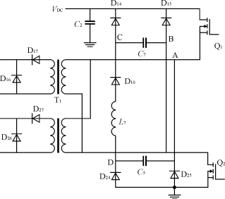
The DC / DC main circuit uses a single-ended double forward circuit. Compared with other topological circuit structures, the single-ended double forward circuit has a low voltage to the switch tube. There is no need to worry about the common mode conduction problem in the design of the control circuit, nor will the unidirectional bias of the high-frequency transformer occur due to the circuit asymmetry There is a transformer saturation problem, which is a circuit with high reliability. Considering that the height of the whole machine does not exceed 60mm, as well as the requirements of transformer technology, installation and heat dissipation, the DC / DC conversion adopts a dual transformer and dual output inductance structure. The primary side of the transformer is connected in parallel, and each secondary side uses an output inductor, as shown in Figure 4.

Figure 4 Double forward excitation lossless absorption main circuit
The lossless absorption network of this circuit is different from the lossless absorption network used by some AC / DC circuits. It only makes the switch tube complete the zero-voltage shutdown process. The following uses switch Q2 as an example (Q1 and Q2 change in the same state) to briefly describe the working principle of the network.
1) Guide through
When Q1 and Q2 are turned on, in addition to one current passing through Q1, T1 secondary side and Q2, the other current flows through Q1, C5, L7, D10, C7 and Q2 to form an LC oscillation circuit, and C5 and C7 are charged. When the voltage uAB between points A and B is equal to the main circuit voltage VDC, due to the unidirectional conductivity of D10, the oscillation ends. Inductor L7 serves to limit the current changes in C7 and C5. The current flowing in Q1 and Q2 is the sum of the load current converted from the secondary side to the primary side and the charging current of C5 and C7.
2) Shutdown process
When Q1 and Q2 are turned off, since the voltage at point B is zero, C7 starts charging from zero, the voltage uQ2 of Q2 rises slowly, and the zero voltage of Q2 is turned off. The voltage applied to Q2 is finally VDC due to the clamping effect of diode D15. Therefore, the voltage at point B rises to VDC. Q2 implements a zero-voltage shutdown process.
The energy of the induced potential caused by the transformer magnetizing inductance, leakage inductance and lead parasitic inductance returns to the power supply through C7 and D14, and the voltage on Q2 is maintained at VDC until the transformer primary side magnetic flux is reset. At this time, the voltages on Q1 and Q2 are VDC / 2 until the new duty cycle.
The state of Q2 during the turn-on period and the turn-off period is the same as the state of the ordinary switch tube during the same period.
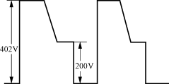
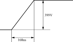
Figure 5 shows the measured Q2 switching waveforms. Figure 6 shows the measured Q2 zero-voltage turn-off waveform.

Figure 5 Q2 D-S pole switching waveform

Figure 6 Q2 turn-off time
From the above analysis, the following characteristics can be summarized.
1) The maximum working voltage of each switch in the circuit is equal to the power supply voltage.
2) The rate of voltage rise when Q1 and Q2 are turned off depends on the capacitance of capacitors C5 and C7, respectively.
2. 3 control circuit design
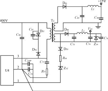
In order to ensure the safe and reliable operation of the power supply, TOP224Y is used in the circuit design to make a flyback switching power supply as an auxiliary source, as shown in Figure 7. Its two outputs provide power for the control circuits of the AC / DC part and the DC / DC part.

Figure 7 Auxiliary power circuit
The AC / DC control part uses the PFC control chip UC3854B. UC3854 is turned off when the AC input is over-voltage, under-voltage, PFC conversion DC voltage (400V) over-voltage or under-voltage, so that the PFC part stops working. These fault signals are transmitted to the DC / DC control circuit through the isolation optocoupler to achieve the purpose of protecting the main switch tube when the AC / DC part is not working properly.
The DC / DC control part uses the PWM control chip UC3846, which adopts the peak current type control mode. Compared with the voltage control mode, the peak current control mode has a fast load response rate, has a pulse-by-pulse current limiting characteristic, and it is easy to obtain the current limiting characteristic of the drag shape, which is very suitable for this application.
When n + 1 redundant application, multi-module must have current sharing function. The output current of the power supply is large, and the power loss of the current signal taken directly from the DC output shunt is large, and the assembly process is complicated. Therefore, this design adopts the method of primary side current synthesis.
Use the current sensor to take out the current signal on the primary side of the transformer when the switch is on. This signal contains the transformer excitation current signal and the output inductor current converted to the transformer primary current signal. Because the current converted from the output inductance to the primary side is much larger than the excitation current of the transformer, it can be considered that what the current sensor takes out is the magnetizing current of the output inductance. This is the rising part of the output inductor current, as long as the falling part of the output inductor freewheel is simulated, the current signal of the output inductor can be obtained after synthesis, which is also the output current signal. After taking out the synthesized current signal, it can be used for current protection control and current sharing control.
If you want to know more, our website has product specifications for capacitor, you can go to ALLICDATA ELECTRONICS LIMITED to get more information

