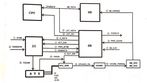
The working principle of AMD RS880 chipset motherboard
The AMD RS880 chipset motherboard works as shown in figure 1.

Figure 1 schematic diagram of the AMD chipset motherboard.
The AMD RS880 chipset motherboard works as follows.
(1)Plug in the power output 5VSB to power the IO chip.
(2)The 5VSB provides standby power to the South Bridge chip by reducing the voltage of the S5 / 3.3V via the circuit.
(3)The IO chip sends out a RSMRST# signal, sent to the South Bridge chip to indicate that the motherboard standby power supply is normal.
(4)Press the switch to generate trigger signal PANSWH # to the IO chip.
(5)The IO chip converts and sends out the PWR_BTN# signal and sends it to the South Bridge chip to request power.
(6)The South Bridge chip sends out a continuously high-level SLP_S5# signal.
(7)The South Bridge chip continues to have a high level of SLP_S3# signal to the 1O chip, indicating that power is allowed.
(8)The IO chip forwards a continuously low-level PSON# signal to the ATX power supply.
(9)The green cable of the ATX power supply is pulled down and the output is + 12V, + 5V, + 3.3V main power supply.
(10)ATX power delay sends out a high-level PWOK signal, and after the SLP_S5# signal is sent to the EN pin of the memory-powered chip, the memory-powered chip is turned on and the output memory-powered VCC _ DDR. is controlled.
(11)The memory power supplies the CPUVDD_EN signal through the conversion, sends to the EN pin of the power management chip, turns on the power management chip to work, controls the voltage step down to get the VCORE power supply to the CPU.
(12)VCORE voltage stabilized output VCORE_ PWROK high level, control bridge power supply circuit works, output SB_VCC and NB_VCC to supply the South Bridge chip and North Bridge chip.
(13)The PWR_ GOOD and NB_PWROK signals are obtained by circuit conversion and sent to the South Bridge chip and the North Bridge chip, respectively, indicating that the main board power supply is normal.
(14)South Bridge chip power supply, clock signal is normal, received PWR_GOOD signal; send a high-level LDT_PG signal to the CPU, to indicate the motherboard is normal.
(15)The South Bridge chip sends out the reset signal of A RST# platform and reset the IO chip.
(16)The South Bridge chip generates a PCIRST# signal and resets the PCI slot.
(17)The South Bridge chip sends out LDT_RST# signals, all of which are renamed as NB_ RST# reset North Bridge Chip and another Road renamed CPURST# reset CPU.
This article is from Allicdata Electronics Limited. Reprinted need to indicate the source.

