What is the three-layer stacking technology of Sony's image sensor?
This Sony patent can make full use of the area below the pad hole, and can increase the utilization efficiency of the substrate compared with the traditional three-layer stacked structure solid-state imaging device. In addition, in the second semiconductor substrate or the third semiconductor substrate, a metal element constituting a measurement terminal is placed, and the first semiconductor substrate is stacked after performing a predetermined measurement, so the measurement time can be greatly reduced.
When it comes to photography, everyone will think of Sony, one of the world's highest-selling camera brands. Of course, the continuous development of Sony cameras will definitely require the innovation of its image sensor technology.
In recent years, solid-state imaging devices (such as CMOS image sensors, etc.) have been widely used in digital cameras, digital video cameras, and the like. Although the three-layer stack structure is the current more advanced image sensor structure, it also has some problems. For example, in the process of opening the deep pad, the resist will thicken, and the resist will be cured after dry etching. Moreover, in the pad opening area in the second layer or below, wiring or circuit elements cannot be arranged, otherwise many dead areas will be generated. In addition, for the existing structure, when performing measurement operations, problems such as an increase in the defect rate and an increase in measurement time will also occur.
To this end, Sony applied for an invention patent entitled "Solid-state imaging device, solid-state imaging device manufacturing method and electronic equipment" (application number: 201580019325.7), the applicant is Sony.

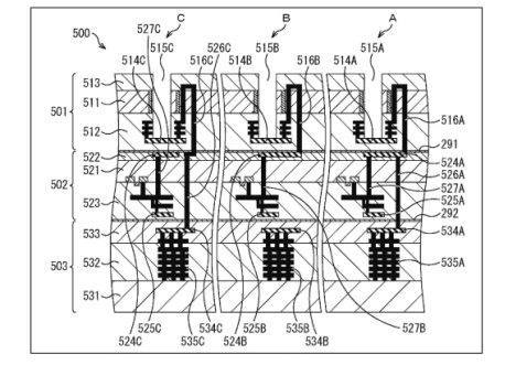
Figure 1 Connection structure diagram in a solid-state imaging element with a three-layer stack structure
FIG. 1 is a connection structure diagram of a solid-state imaging element with a three-layer stacked structure proposed by this invention. It can be seen from the figure that a solid-state imaging element 500 is stacked by a first layer substrate 501, a second layer substrate 502, and a third layer substrate 503. The resulting three-layer stacked structure is constructed. Among them, a sensor circuit, a logic circuit and a memory circuit are sequentially arranged between the three-layer structure.
In the first layer substrate 501, the wiring layer 512 and the planarization film 513 are stacked on the surface side and the back surface side of the silicon substrate 511, respectively. Also, the pad hole 515 penetrates the first layer substrate 501 from the back side and forms an aluminum pad 514 in the wiring layer 512.
Next is the second layer substrate 502, the wiring layer 522 is stacked on the back side of the silicon substrate 521, while the wiring layer 523 is stacked on the surface side of the silicon substrate 521. In the second layer substrate 502, the wiring layers 522 and 523 are respectively formed with an aluminum pad 524 on the back side and an aluminum pad 525 on the front side. Since the substrate is located between the three-layer stack structure, the contact portion 526 can be used to connect the first substrate 501 and the third substrate 503. In addition, the second layer substrate 502 also has aluminum pads 524 on the back side, aluminum pads 525 on the front side, and contact portions 527. These contacts can be connected to form the logic in the second layer substrate 502. The transistor of the circuit.
Finally, there is the third-layer substrate 503, which is configured such that the wiring layer 532 is stacked on the surface side of the silicon substrate 531, and the wiring layer 533 is stacked on the wiring layer 532. In addition, the wiring layer 533 forms an aluminum pad 534, and the wiring layer 532 also includes a connection conductor 535 for connecting the memory circuit in the third layer substrate 503.
Viewed as a whole, the first and second-layer substrates and the second and third-layer substrates are bonded by bonding surfaces 291 and 292, respectively, to form a solid-state imaging element 500.
This Sony patent can make full use of the area under the pad hole, and can increase the utilization efficiency of the substrate when compared with the traditional three-layer stacked structure solid-state imaging device. In addition, in the second semiconductor substrate or the third semiconductor substrate, a metal element constituting a measurement terminal is placed, and the first semiconductor substrate is stacked after performing a predetermined measurement, so the measurement time can be greatly reduced.
In terms of the volume of CMOS that can be used in smartphones, Sony’s three-layer stack structure has improved the picture quality to the extreme that can be achieved under structural and volume constraints. So what will Sony do in the future on image sensors? let us wait and see.
If you want to know more, our website has product specifications for image sensor, you can go to ALLICDATA ELECTRONICS LIMITED to get more information

