How to solve the problem of conducted EMI?
EMI means that the work of electronic products will cause interference to other electronic products in the surroundings, and related to this is the EMC specification. Is often encountered in electronic and electrical products. The types of interference are conducted interference and radiated interference. Currently, most conducted EMI problems are caused by common-mode noise. Moreover, most common-mode noise problems are caused by parasitic capacitance in the power supply. The following will focus on what happens when parasitic capacitance is directly coupled to the power input wires.
1. Only a few fF stray capacitance will cause the EMI scan to fail. Essentially, switching power supplies have nodes that provide high dV / dt. Mixing parasitic capacitance with high dV / dt can cause EMI problems. When the other end of the parasitic capacitor is connected to the power input, a small amount of current is pumped directly to the power line.
3. There are techniques to reduce the surface area. Try to use surface mount packages whenever possible. The FET in the vertical TO-220 package has a large drain tab surface area. Unfortunately, it usually happens to be the node with the highest dV / dt. Try using surface mount DPAK or D2PAK FET instead. Placing a primary ground plane on the low-level PCB under the DPAK tab provides good shielding of the bottom of the FET, which can significantly reduce parasitic capacitance.
2. Look at the parasitic capacitance in the power supply. We all remember from the physics class that the capacitance between two conductors is proportional to the surface area of the conductor and inversely proportional to the distance between them. Look at each node in the circuit and pay special attention to the nodes with high dV / dt. Think about the surface area of the node in the circuit layout and how far the node is from the board's input line. The drain and snubber circuits of switching MOSFETs are common culprits.
Sometimes the surface area is needed for heat dissipation. If you must use a TO-220 class FET with a heat sink, try connecting the heat sink to the primary ground instead of the earth ground. This not only helps to shield the FET, but also helps reduce stray capacitance.
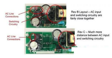
4. Keep the distance between the switch node and the input connection. See the design example in Figure 1 where I overlooked this simple principle.

Figure 1: Having input wiring too close to nodes with high dV / dt increases conducted EMI.
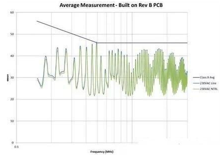
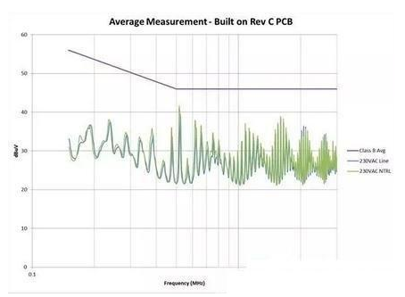
I simply adjusted the board (no circuit changes) and reduced the noise by about 6dB. See Figure 2 and Figure 3 for the measurement results. In some cases, routing input lines close to high dV / dt can even damage the common mode coil (CMC).

Figure 2: EMI scan from board layout, where the AC input is closer to the switch circuit

Figure 3: EMI scan from board layout, where the distance between the AC input and the switching circuit is large
Have you ever encountered such a problem that the EMI improvement effect is very small or not improved after significantly strengthening the input filter? This is most likely because some stray capacitance from a high dV / dt node is directly coupled to the input line, effectively bypassing your CMC. To detect this, temporarily short the windings of the CMC on the PCB and connect a secondary CMC in series with the input wires of the board. If there is a noticeable improvement, you need to re-lay out the board and pay special attention to the layout and routing of the input connections.
If you want to know more, our website has product specifications for the EMI, you can go to ALLICDATA ELECTRONICS LIMITED to get more information

