What is reflow and how does reflow affect capacitor signal integrity?
What is reflow? How does reflow affect signal integrity? Please see the example below.
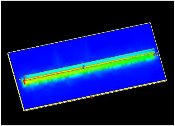
Reflow distribution of microstrip lines
The example of reflow
First observe a phenomenon, as shown in the following figure, for a typical 4-layer plate structure, the signal is changed from the first layer through the hole to the fourth layer, and the corresponding reference plane is switched from the second layer to the third layer. This is often the case when designing Layout.
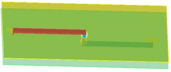
4-layer laminate structure
Let us first look at the S-parameter. As the frequency increases, the return loss S11 becomes worse and worse, especially after 10 GHz, which is -16.2 dB, which is less than -20 dB.
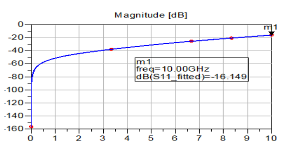
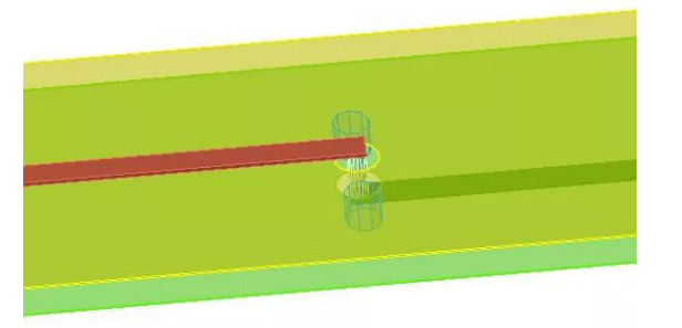
When the accompanying ground hole is added next to the signal via, its S11 reaches -28.3 dB at 10 GHz, which indicates that the high speed performance is improved.
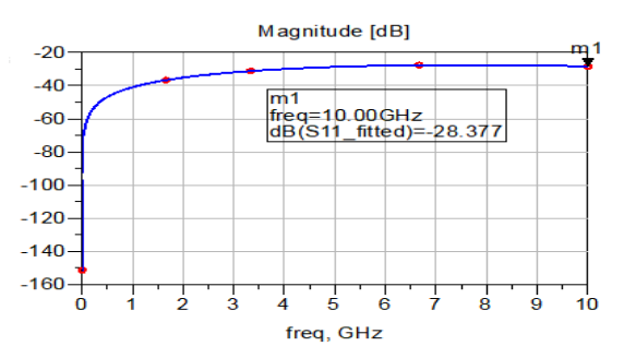
This is why many high-speed electrical PCB design rules require "the need to play with the ground hole when changing high-speed signals."
So why does the performance at high frequencies improve after the hole is added?
Since S11 reacts to the impedance characteristics of the signal, it means that the impedance characteristics at high frequencies are deteriorated without increasing the associated hole, and the impedance characteristics become better after the hole is added. Then why? Today we explain the impedance characteristics from the perspective of reflow.
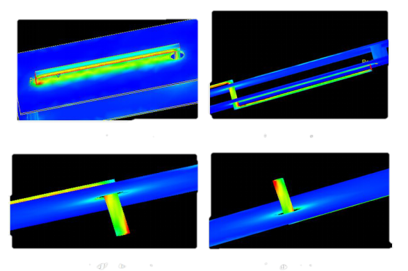
A transmission line model is formed between 1 and 2, 3 and 4, and the return current still satisfies the reflow characteristics of the microstrip line. We focus on the return current distribution between 2 and 3. When without accompanying the ground hole, the current density distribution of the lower surface of layer 2 and the upper surface of layer 3 is as follows:
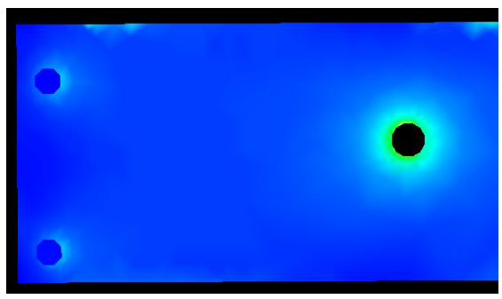
F=3.3GHz
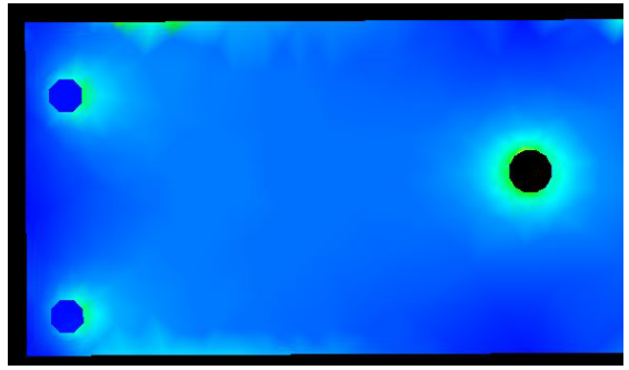
F=10GHz
It can be seen from the figure that the reflow on the ground plane is mainly distributed in a small area around the via at 3.3 GHz, and at 10 GHz, the reflow on the ground plane is not only distributed around the via, but further extended to more In the distance, this means that the path of returning is longer.
When two associated holes are added next to the signal hole, the current density distribution on the reference layer is as shown below:
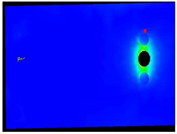
F=3.3GHz
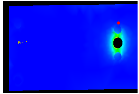
F=10GHz
It can be seen from the figure that at 3.3 GHz and 10 GHz, the current density is concentrated between the signal via and the accompanying via, no longer like external diffusion, which changes the path of the reflow, so that at high frequencies, reflow The path becomes shorter and the parasitic inductance on the path becomes smaller. At this time, the role of the ground hole is to provide a shortest return path when switching the reference plane. This is also the reason why the hole is sometimes called the backflow hole.
![]()
![]() In order to further understand the distribution of the above reflow, let's take a look at the equivalent single way angle. As shown in the figure below, the direction of the return flow on the reference plane when the signal is changed.
In order to further understand the distribution of the above reflow, let's take a look at the equivalent single way angle. As shown in the figure below, the direction of the return flow on the reference plane when the signal is changed.
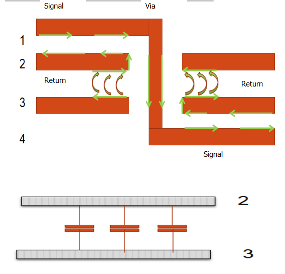
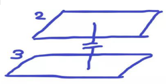
As can be seen from the figure, for the 1-2 layer, the flow of the return current flows in addition to the upper surface of the reference plane 2, and there is also a small flow of current on the lower surface; likewise, for the 3-4 layer The flow of the return current flows in addition to the lower surface of the reference plane 3, and there is also a small flow of current on the upper surface; this is not the same as the simple microstrip line reflow. This difference is caused by changing the layer through the hole.
The current between 2-3 flows through the plate capacitance formed by the plane between 2 and 3. We know that a plate capacitor is formed between the overlapping areas of the two planes, so a lot of parasitic capacitance effect is formed between the inner layers of 2-3. When the reference layer of the signal is switched, the return current spreads along the distance of the plane. It is related to the layer structure of the board, and also related to the frequency of the signal. From the simulation of the above figure, the higher the frequency, the more the diffusion is, which is also the high-frequency signal always has to go the embodiment of the lowest path.
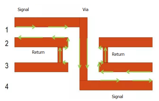
When the associated hole is added, the current flow between 2 and 3 can be directly returned through the via, no need to return through the physical structure of the plate capacitor, and the return current no longer spreads further along the plane, which controls the path of the reflow is such that even at high frequencies, the return current can be returned in the shortest path without affecting the impedance.
If you want to know more, our website has product specifications for the capacitor, you can go to ALLICDATA ELECTRONICS LIMITED to get more information

