Texas Instruments: What is an operational amplifier?
Many textbooks and reference guides define operational amplifiers (op amps) as application specific integrated circuits (ICs) that can perform various functions or operations (such as amplification, addition, and subtraction). Although I agree with this definition, it is still necessary to pay attention to the voltage of the input pins of the chip.
When the input voltage is equal, the operational amplifier usually works in the linear range, and the operational amplifier precisely performs the above function in the linear range. However, the operational amplifier can only change one condition to make the input voltage equal, that is, the output voltage. Therefore, the output of an op amp is usually connected to the input in some way, which is often referred to as voltage feedback.
In this article, I will explain the basic operation of a general-purpose voltage feedback operational amplifier, and please refer to other contents for more information.
Operational amplifier design
Figure 1 depicts the standard schematic symbols of an operational amplifier. There are two input terminals (IN +, IN-), one output terminal (OUT) and two power terminals (V +, V-). The names of these terminals may vary by manufacturer, and even a single manufacturer may use different names, but they are still the same five terminals.
For example, you may see Vcc or Vdd instead of V +. Or, you might see Vee or Vss instead of V-. The other labels of the power terminals will be different because they refer to the type of transistor inside the device. For example, when using a bipolar junction transistor (BJT) inside an operational amplifier, the power supply corresponds to the collector and emitter of the BJT: Vcc and Vee. When using field effect transistors (FETs) inside the op amp, the power supply label corresponds to the drain and source of the FET: Vdd and Vss. Today, many op amps contain both BJT and FET, so V + and V- are common tags, regardless of the transistors inside the device. In short, don't care too much about pin labels, just understand their role.
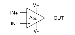
Figure 1: Schematic symbols of general-purpose operational amplifier
Equation 1 represents the transfer function of the operational amplifier:

In Equation 1, AOL is called "open-loop gain." In modern operational amplifiers, it is usually a very large value (120 dB or 1,000,000 V / V). For example, if the voltage difference between IN + and IN- is only 1mV, the operational amplifier will try to output 1000V! In this configuration, the op amp does not work in the linear region because the output cannot equal the inputs to each other (remember, ideally In + equals In-). Therefore, the operational amplifier needs a way to control the open-loop gain, that is, through negative feedback.
Figure 2 depicts the operational amplifier as part of the feedback control system. You will notice that the output OUT is fed back to the negative input IN- through a block labeled ß. ß is called the feedback factor and usually uses resistors to reduce the output voltage.
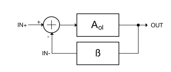
Figure 2: Negative feedback operational amplifier
Figure 3 compares the open-loop operational amplifier and the negative feedback operational amplifier. The op amps used in these TINA-TI ™ software emulation circuits are near-ideal op amps, with power supplies added to limit the output voltage. Note that for the open-loop configuration on the left, the output is almost equal to the positive power supply (V +). This is because there is a small difference (100mV) between the input pins. This small voltage is amplified by the open-loop gain, which will force the output to one of the supply voltages. In the negative feedback or closed-loop circuit on the right side of Figure 3, the voltage divider on the output of the operational amplifier requires an output voltage of 200 mV in order to equalize the inverting and non-inverting inputs.
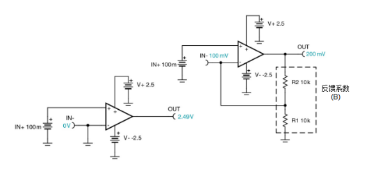
Figure 3: Open loop (left) and negative feedback (right)
The amplification of the input voltage is called the gain. It is a function of the resistance value in the feedback loop. Equation 2 describes the gain equation of the circuit on the right in Figure 3, which is called a non-inverting amplifier. You will see that the calculated output voltage matches the simulation. If you want to learn more about this circuit (as well as other common operational amplifier circuits such as buffers, non-inverting amplifiers, and differential amplifiers), you can download the eBook "Analog Engineer Circuit Guide: Amplifiers". "

The output of the operational amplifier is limited by the power supply voltage. FIG. 4 is a relationship diagram between the output voltage and the input voltage of the non-inverting amplifier in FIG. 3. Note that when the output is close to a positive or negative power supply, the output is limited due to saturation.
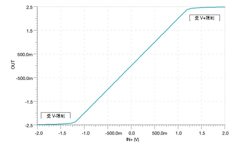
Figure 4: Output and input voltage of non-inverting amplifier circuit
Due to this limitation, it can be seen in FIG. 5 that as the output approaches the power supply, the voltage difference Vdiff between the input pins increases. Only when the inputs are almost equal, the operational amplifier operates in the linear region.
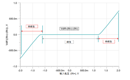
Figure 5: Vdiff and IN + of the in-phase amplifier circuit
For a deeper understanding of operational amplifiers, please view our analog course TI High Precision Laboratory. This course will delve into operational amplifiers and discuss basic non-ideal factors such as input offset voltage (Vos), input bias current (IB), and input / output limits. There are also lectures on advanced topics such as operational amplifier bandwidth (BW), slew rate (SR), noise, common-mode rejection ratio (CMRR), power supply rejection ratio (PSRR), and stability. In addition to lectures, some topics include hands-on experiments. In order to carry out these experiments, you need the corresponding op amp evaluation module.
If you like DIY circuits, you may evaluate the general-purpose DIY amplifier circuit evaluation module (for single-channel op amps), the dual-channel general DIY amplifier circuit evaluation (for dual-channel op-amps), or the DIP package conversion evaluation module (available with Standard proofing board or circuit breadboard used together) interested. DIY-EVMs support op amps in different packages, and have many standard op amp circuits, such as non-inverting amplifiers, inverting amplifiers, buffers, and filters (including Sallen-Key and multiple feedback) as described in this article. Because the dual in-line package (DIP) conversion EVM can convert many standard surface mount packages to DIP for use with circuit breadboards, you can evaluate any configuration of amplifier.
This is the basic principle of the operational amplifier: only when the voltage of the input pin is equal, the operational amplifier is linear. However, to achieve this, the op amp can only adjust its output voltage. The output swing limit will cause the input voltage difference to increase, resulting in non-linearity.
If you want to know more, our website has product specifications for amplifier, you can go to ALLICDATA ELECTRONICS LIMITED to get more information

