What are the tips for selecting TVS?
(1) Determine the maximum DC or continuous working voltage of the protected circuit, the rated standard voltage of the circuit and the "high-end" tolerance.
(2) TVS rated reverse turn-off VWM should be greater than or equal to the maximum working voltage of the protected circuit. If the selected VWM is too low, the device may enter an avalanche or affect the normal operation of the circuit due to excessive reverse leakage current. The serial connection divides the voltage, and the parallel connection divides the current.
(3) The maximum clamping voltage VC of TVS should be less than the damaged voltage of the protected circuit.
(4) Within the prescribed pulse duration, the maximum peak pulse power consumption PM of the TVS must be greater than the peak pulse power that may appear in the protected circuit. After the maximum clamping voltage is determined, its peak pulse current should be greater than the transient surge current.
(5) For the protection of the data interface circuit, we must also pay attention to the selection of TVS devices with appropriate capacitance C.
(6) Select the polarity and packaging structure of TVS according to the application. It is more reasonable to choose bipolar TVS for AC circuit; it is more advantageous to choose TVS array for multi-line protection.
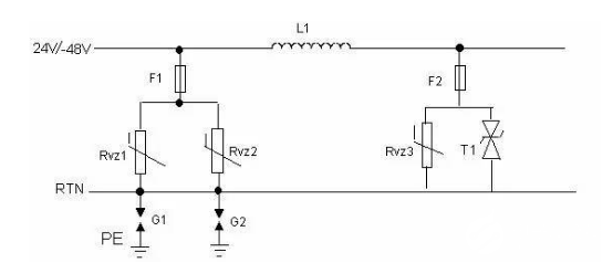
(7) Temperature considerations. The transient voltage suppressor can work between -55 ℃ ~ + 150 ℃. If the TVS is required to work at a varying temperature, its reverse leakage current ID increases with increase; the power consumption decreases with the increase of the TVS junction temperature, from + 25 ℃ to + 175 ℃, approximately linearly decreases by 50% The voltage VBR increases with a certain coefficient as the temperature increases. Therefore, the relevant product information must be consulted to consider the effect of temperature changes on its characteristics. The best way to deal with the damage of the transient pulse to the component is to divert the instantaneous current from the sensing element. The TVS diode is connected in parallel with the protected circuit on the circuit board. When the instantaneous voltage exceeds the normal operating voltage of the circuit, the TVS diode generates an avalanche, providing an ultra-low resistance path to the instantaneous current. The result is that the instantaneous current is diverted through the diode. Avoid the protected element, and keep the protected circuit at the cut-off voltage until the voltage returns to the normal value. When the transient pulse ends, the TVS diode automatically returns to the high-impedance state, and the entire loop enters normal voltage. After many components are subjected to multiple shocks, their parameters and performance will be degraded, and as long as they work within the limits, the diode will not be damaged or degraded.
It can be seen from the above process that when selecting TVS diodes, attention must be paid to the selection of the following parameters:
1. The minimum breakdown voltage VBR and breakdown current I R. VBR is the minimum breakdown voltage of TVS. At 25 ° C, TVS will not produce an avalanche below this voltage. When the TVS flows through the specified 1mA current (IR), the voltage applied to the two poles of the TVS is its minimum breakdown voltage V BR. According to the dispersion degree of TVS VBR and standard value, VBR can be divided into 5% and 10%. For 5% VBR, V WM = 0.85 VBR; for 10% VBR, V WM = 0.81 VBR. In order to meet the IEC61000-4-2 international standard, TVS diodes must be able to handle a minimum of 8kV (contact) and 15kV (air) ESD shocks. Some semiconductor manufacturers use higher shock resistance standards in their products. For some portable device applications with special requirements, designers can select components as needed.
2. Maximum reverse leakage current ID and rated reverse cut-off voltage VWM. VWM is the voltage that the diode can withstand in a normal state. This voltage should be greater than or equal to the normal working voltage of the protected circuit, otherwise the diode will continuously cut off the loop voltage; but it needs to be as close as possible to the normal working voltage of the protected loop. It will not make the entire circuit face the threat of overvoltage before TVS works. When this rated reverse cutoff voltage VWM is applied between the two poles of the TVS, it is in the reverse cutoff state, and the current flowing through it should be less than or equal to its maximum reverse leakage current ID.
3. The maximum clamping voltage VC and the maximum peak pulse current I PP. When a pulse peak current IPP with a duration of 20 ms flows through the TVS, the maximum peak voltage appearing across it is VC. V C and IPP reflect TVS's surge suppression capability. The ratio of VC to VBR is called the clamping factor and is generally between 1.2 and 1.4. VC is the voltage provided by the diode in the off state, that is, the voltage that passes through the TVS during the ESD shock state. It cannot be greater than the tolerable limit voltage of the protected circuit, otherwise the component is in danger of being damaged.
4. Pppm rated pulse power, which is based on the maximum cut-off voltage and the peak pulse current at this time. For handheld devices, generally 500W TVS is sufficient. The maximum peak pulse power consumption PM is the maximum peak pulse power consumption value that the TVS can withstand. Under a certain maximum clamping voltage, the greater the power consumption PM, the greater its ability to withstand surge current. Under a specific power consumption PM, the lower the clamping voltage VC, the greater its ability to withstand surge current. In addition, the peak pulse power consumption is also related to the pulse waveform, duration and ambient temperature. Moreover, the transient pulses that TVS can withstand are not repeated, and the pulse repetition frequency (ratio of duration to pause time) specified by the device is 0.01%. If repeated pulses appear in the circuit, the accumulation of pulse power should be considered, which may damage the TVS.
5. The amount of capacitor C. The amount of capacitor C is determined by the TVS avalanche junction cross section and is measured at a specific frequency of 1 MHz. The size of C is proportional to the current withstand capability of the TVS. If C is too large, the signal will be attenuated. Therefore, C is an important parameter for the selection of TVS for data interface circuits. The higher the data / signal frequency of the capacitor, the greater the interference of the diode capacitor on the circuit, which forms noise or attenuates the signal strength. Therefore, the capacitor range of the selected component needs to be determined according to the characteristics of the loop. High-frequency loops generally choose capacitors as small as possible (such as LCTVS, low-capacity TVS, capacitors are not greater than 3pF), and loop capacitors that do not require high capacitors can be selected above 40pF. TVS diode characteristic curve:

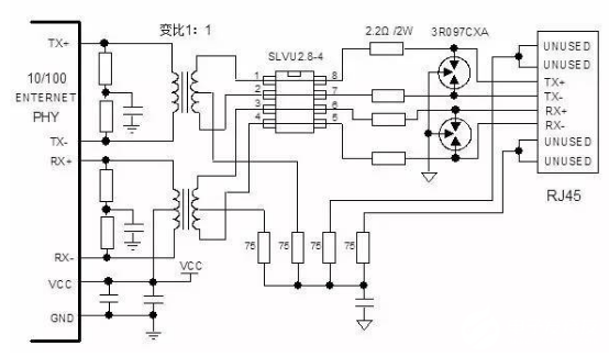
Outdoor network port protection circuit

Note that the parasitic capacitance of the TVS tube may affect signal integrity. A varistor can be placed on the tap of the transformer as a protective circuit to support a higher-speed network port design.
485 protective circuit design

If you want to know more, our website has product specifications for TVS, you can go to ALLICDATA ELECTRONICS LIMITED to get more information

