How to realize high-speed programmable large array two-dimensional optical phased array chip?
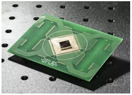
The results of the MEMS expert team from the University of California, Berkeley (Berkeley) achieved the first high-speed programmable, large array of 2D Optical Phased Array (OPA) chips. Compared with traditional OPA technology such as silicon light and liquid crystal, the chip innovatively combines the new grating structure with silicon-based MEMS technology, which has the advantages of more economy, higher speed and higher reliability.

In addition, the optical modulation of the MEMS OPA is done in free space, enabling optical coupling without insertion loss. In particular, the grating structure can be applied to the broadband spectrum from visible light to near-infrared, and is not limited by the integrated wavelength on the silicon light sheet, so it can be directly applied to a wide range of medical imaging equipment, optical communication and holographic television. The field and the more powerful Lidar (LiDAR) sensors for autonomous vehicles.
The concept of optical phased arrays has been proposed for decades and is currently used in medical imaging and optical communications. The idea of Berkeley researchers is to construct an array of light emitters and to obtain a source that has no physical motion but can emit a laser beam in any direction by changing their phase or by changing the arrangement of the light waves they produce. This flexible beam deflection is very useful in LiDAR technology. LiDAR determines the distance of nearby objects by emitting laser beams in all directions and measuring the time it takes to return.
Today, the most widely used LiDAR is a mechanical rotary LiDAR sensor mounted on top of an autonomous vehicle, such as the most well-known "family bucket" HDL-64E from Velodyne. This LiDAR is costly to produce and has a worrying reliability because it is not known whether this mechanical rotating mechanism can withstand the daily use of vehicles for many years. This is why many industry experts believe that optical phased arrays are more promising as a solid-state LiDAR technology.
At present, the biggest challenge of optical phased arrays for LiDAR is its relatively slow beam deflection speed, which is a point-by-point scan, and its limited overall aperture, which determines the optical resolution of the system.
In conventional optical phased array designs, spatial light modulators that modulate beam intensity are mostly composed of very small moving parts, so these devices operate only at certain wavelengths and are limited by the scannable range. This limits their efficiency and reliability because their signals are affected by the surrounding environment, especially in environments with rapidly changing temperatures.
To overcome these limitations, the research team developed a silicon-based chip that uses a MEMS actuator to laterally move the grating elements, which diffract light in all directions. This phase shifting motion adds delay to the output laser beam, creating a holographic pattern that directs light into a predefined pattern. This working mechanism is basically similar to a spatial light modulator, enabling researchers to significantly reduce the sidelobe intensity, thereby increasing the optical transmission efficiency of the technique.
Berkeley researchers have made the chip programmable with sophisticated CMOS technology that builds all the basic units of the microprocessor. This means that the user can pre-program different holographic patterns on the chip. By stacking 160 x 160 arrays of fine-tuned polysilicon phase shifters on top of MEMS actuators, researchers were able to reduce beam divergence and increase the number of distinguishable points. This allows the chip to achieve a large field of view and build a high resolution 3D hologram of its surroundings. Furthermore, by using an existing manufacturing process, the manufacturing cost of the chip is lower than that of an optical phased array made of liquid crystal.
The Berkeley researchers achieved a resonant frequency of 55 KHz in the prototype, corresponding to a response time of 5.7 us (the time it takes for an optical phased array to change one holographic pattern into another), which is almost traditionally based. The optical phased array of liquid crystal is 1000 times. The MEMS 2D optical phased array captures high-resolution images of the surrounding environment by utilizing a large array of 25,600 pixels packaged on a 3.1mm x 3.2mm chip.
If you want to know more, our website has product specifications for the high-speed programmable large array two-dimensional optical phased array chip, you can go to ALLICDATA ELECTRONICS LIMITED to get more information

