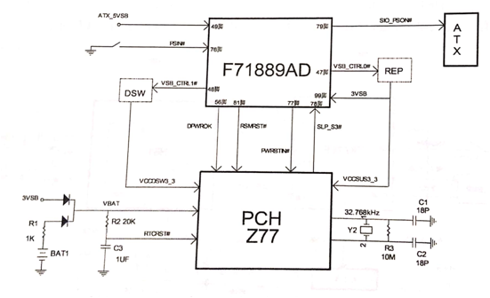
The operating principle of the Intel single-bridge Z77 chipset motherboard boot circuit.
The Intel Z77 chipset supports Windows 7 and Windows 8 systems and no longer supports Windows XP systems. In the Windows 8 system to enter the deep dormancy state, must be supported by the motherboard, so the Z77 chipset began to support the class body sleep state, so that the motherboard should first turn on the deep dormancy power supply and send good signals to the bridge when starting the system board. Causes the motherboard to enter standby, finally enters the boot state. The Intel Z77 chipset motherboard boot circuit works as shown in figure 1.

Figure 1 operating principle block diagram of the motherboard boot circuit of the Intel Z77 chipset.
The Intel Z77 chipset motherboard boot circuit works as follows.
The first stage: battery BATI current limiting through resistance RI into the Schottky transistor positive pole, from the negative output VBAT for the bridge RTC circuit power supply, VBAT through R2 and C3 delay through the RTCRST# high-level multiplex bridge internal real-time clock circuit, the bridge to power the crystal oscillator, Product vibration operation output 32.768kHz frequency to the bridge.
The second stage: plug in the power output ATX 5VSB to power the 49 pins of the F71889AD, and output the DPWROK high level from 56 pin to the bridge to indicate that the deep dormant power supply is normal.
The third phase: the tap switch generates the PSIN# trigger signal to the 76 pins of the F71889AD, and the F71889AD outputs the VSB CTRLO# and VSB CTRL1# signals. The VSB CTRLI# controls the DSW deep sleep power supply circuit to work, generating VCCDSW3 3 to provide the bridge with a deep sleep power supply. VSB_CTRLO# controls ERP circuit output 3VSB to provide standby power to F71889AD and VCCSUS3-3 standby power to PCH. F71889AD gets 3VSB power supply from 81 pin output RSMRST# high level to PCH indicates standby power supply is normal. The F71889AD internal delay sends the PWRBTN# signal of the 3.3V-0V-3.3V jump from 77 pin to power up the PCH request. After the PCH standby condition is good and the power-up request signal is received, the SLP S3 # continues to be high and is sent to the 78-pin of the F71889AD to indicate that the power-up is allowed. Finally, the F71889AD outputs the sustained low level SIO_PSON# signal from the 79 pin to pull down the ATX power supply green cable to complete the power up.
This article is from Allicdata Electronics Limited.

