Intel H61 chipset motherboard reset circuit work principle.
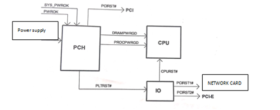
Intel single bridge H61 chipset motherboard reset circuit works as shown in figure 1.

Fig. 1 Working principle block diagram of the reset circuit of Intel single-bridge H61 chipset motherboard.
1.Short switch, the main board circuit starts to work, through the power supply circuit step down to produce the memory power supply, the bridge power supply, the bus power supply and the CPU power supply and so on the voltage.
2. When the power supply of CPU is stabilized, the power management chip outputs high-level VR_RDY signal. After the circuit is converted into SYS _ PWROK bridge, it indicates that the power supply of CPU is normal.
3. After the output voltage of ATX is stable, the output ATX_PWROK signal is delayed to the IO chip. After the internal conversion of the IO chip, the PWROK high level feed bridge is output, which indicates that the power supply of the ATX power supply is normal.
4. Bridge internal clock circuit turned on, for the motherboard equipment to provide clock signal.
5. Bridge power supply, clock signal is normal and receive two PG signals to send DRAMPWRGD signal to CPU, to indicate memory power supply is normal.
6. Bridge re-output PROCPWRGD signal to the CPU indicated that the full board power supply is normal.
7. The bridge sends out the PLTRST# reset signal to reset the IO chip, and the bridge internal delay sends out the PCIRST# reset PCI slot.
8. After receiving the PLTRST# reset signal from the bridge, the IO chip sends out the CPURST# reset CPU, through the internal logic circuit conversion, and sends out the PCIRST1# reset network card chip, and the PCIRST2# resets the PCL-E slot.
This article is from Allicdata Electronics Limited.

