The working principle of reset circuit of AMD RS80 chipset motherboard.
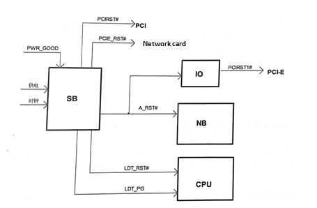
The AMD dual-bridge RSS chipset reset circuit works as shown in figure 1.

Fig. 1 working principle block diagram of reset circuit of AMD dual-bridge RS880 chipset motherboard.
1. The main board power supply circuit step down to get the memory power supply, the CPU power supply, the bridge power supply and the bus power supply.
2. Clock circuit is opened directly by the 3.3 V main power supply, provides the clock signal to the main board equipment.
3. After the power supply of the bridge is normal, a high-level PWR_GOOD signal is generated by circuit conversion, which is sent to the South Bridge chip and the North Bridge chip, indicating that the mainboard power supply is normal.
4. After the South Bridge chip receives the power supply good signal, sends out the LDT_PG signal to the CPU, to indicate the main board power supply is normal.
5. South Bridge chip internal logic circuit conversion output A_RST# reset signal, reset North Bridge chip and IO chip, South Bridge chip internal delay PCIRST# reset PCI slot, PCIE RST# reset network card chip.
6.IO chip through internal conversion circuit output PCIRSTI# reset PCL-E slot card .
7. The South Bridge chip sends out a LDT_RST# signal reset CPU, CPU to start working.
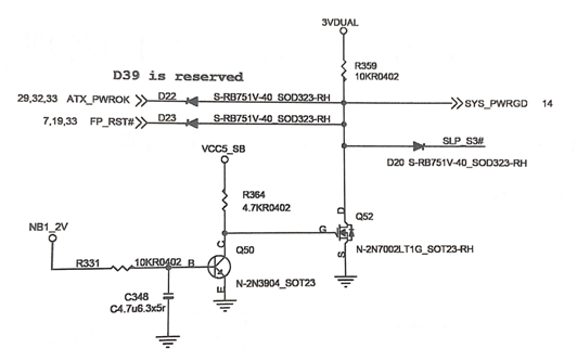
The PWR_GOOD signal generation circuit is shown in figure 2. The PWR GOOD power supply good signal of the AMD motherboard is generated by the bridge power supply and multiple signals generated by the gate circuit. The NB1_2V North Bridge chip power supply is sent to the B board of the Q50 via the resistor R331 so that the Q50 is on and Q52 is cut off. After the ATX power supply is stabilized, the 5 V high level output ATX _ PWROK is fed to the negative pole of the D22 to cut off the D22. Reset switch FP_RST# signal 33V high level feed to D23 negative board to make D23 cut off. The short switch rear bridge chip emits 3.3V SLP_S3# high level to the negative pole of the D20 to cut off the D20. NBI2V, ATX PWROK,FP RST#, SLP_S3# passes through circuit phase and conversion. The 3.3V SYS_PWRGD signal from R359 is sent to the PWR _ GOOD pin of the South Bridge chip, indicating that the power supply of the motherboard is normal.

Fig. 2 PWR_GOOD signal generation circuit.

