The working principle of RT9214 chip is analyzed.
The Intel platform has fully supported DDR2 memory since the 915 chipset and can support dual channels with memory capacity up to 4GB. The speed of data processing in memory is improved and the amount of data is increased, which makes the memory require higher power supply current and power supply stability. Therefore, most of the motherboards using DDR2 memory use switching power supply to provide high-current, high-voltage power supply for memory. The common memory power supply control chips are RT9202, RT9214, W83321, 1SL6520, APW7120, RT8105, ISL6545, NCP1587 and so on. Their functions and pin definitions are different, but the working principle is the same. Take RT9214 chip as an example to analyze the principle of DDR2 memory power supply.
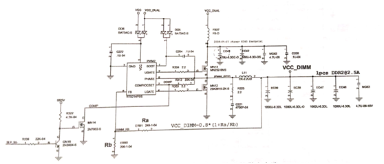
The power supply circuit for the RT9214 chip to control the DDR2 memory is shown in figure 1, and its working process is as follows.

Figure 1. The RRT7214 chip controls the power supply circuit of the DDR2 memory.
1. VCC supplies R72144 chips with 5-pin power via diode DD6 and VCC_DUALsupplies RT9214 chip pins with Schottky diode .
2. The short switch sends the trigger signal to the South Bridge chip to request power, and the South Bridge Chip sends out a high level SLP _ S5-signal through the resistor R336 to the B pole of the Triode QN16 so that the Triode QN16 is on and the MOS transistor MN14 is cut off. RT9214 chip 7 feet through the internal pull-up to get more than 0.4V high level, turn on the chip to work.
3. RT9214 chip outputs signal from 2 pins to make upper tube MN13 on, VCC_DUAL charges L11, EC39 and other energy storage elements through MN13, and outputs VCC_DIMM power.
4. VCC_DIMM power is fed through a split-voltage sampling circuit consisting of ER91 and ER9O, fed back to the chip's 6-pin comparator with an internal 0.8V reference voltage.
5. When the voltage returned to the RT9214 chip 6 pin is higher than 0.8V, the chip 2 pin output signal closes the upper tube MN13. From the 4-pin output signal driven under the tube MNI2 conduction, forming a circuit to let inductance and capacitance discharge, power supply to the later stage.
6. When the 6-pin voltage of the RT9214 chip is less than 0.8V, turn on the upper tube again to charge the LII, EC39, and other components, and then output the voltage again.
7. 3-6-step cycle operation, then output stable VCC_DIMM power supply through capacitive filter.

