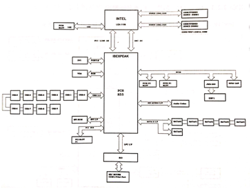
DDD Intel H555 chipset I3 Series motherboard architecture
Intel chipset from the G41 chip behind the use of dual bridge integrated 5 series chipset. Also on the first generation of Intel single-bridge chip, referred to as PCH. The 5 series chipsets include P55, H55, P57, B57.
The Intel H55 chipset motherboard architecture is shown in figure 1.

Figure 1 Intel H5 chipset motherboard architecture.
The management and support functions of the Intel H55 chipset motherboard are as follows.
1.H55 chipset supports the first generation of Intel 13 processors using 1156-pin CPU,. Starting with the 13 series。
2.Intel processor integrates the graphics and memory controllers internally, while the processor and the bridge are connected using the FSB bus instead of the FDI bus and the DMI bus. The FDI bus is responsible for the display data transmission between the display card controller and the bridge, and the DMI bus is responsible for the control signal transmission between the processor and the bridge, which is equivalent to the data between the two-bridge South Bridge chip and the North Bridge chip. CPU also manages the PCI-E X16 standalone video card slots. 1156-pin CPU internal integrated memory controller, memory from the previous North Bridge chip management to CPU management, which can improve the speed of CPU to read memory data.
3.Intel single bridge chip is divided into H and P series. H series bridge integrated display output module, can directly output video signals, can be understood as centralized display. P-Series Bridge does not integrate the display output module, can be understood as a single display, to output the display signal must be attached to a separate video card.
4.H55 chipset motherboard has only one bridge PCH, bridge is responsible for managing devices other than memory, such as VGA and DVI display output interface, USB2.0 interface, sound card chip, SATA hard disk interface, PCI slot.The bridge connects 8-pin BIOS chip through SPI bus, and manages PCL-E XI, Nic chip and JMB-368 IDE interface converter through PCL-E bus.
5.The IO chip connects the bridge through the LPC bus, while the IO chip manages the input / output interfaces such as keyboard, mouse, serial port, parallel port, fan and so on.
This article is from Allicdata Electronics Limited. Reprinted need to indicate the source.

