Memory VTT power supply circuit analysis.
Memory load powered (VTT_DDR), for memory and memory controller (North Bridge chip or CPU) between the data address line pull-up, stable signal transmission. VTT_ DDR power supply generally uses RT9173, RT9199, W83310, APL5336, UP7711 special chip. The RT9199 physical is shown in figure 1, and the pin definition is shown in figure 2.

Figure 1 RT9199 physical diagram. Figure 2 RT9199 pin definition diagram.
RT9199 and other chips use two external resistors to divide the input voltage to get the reference voltage. It contains high-speed operational amplifier, fast response speed, high precision voltage stabilization, well and output short-circuit protection and over-heat protection and other functions. When the device is used without inductor or output filter capacitance, it can reduce the number of components, save the system design space, and facilitate the design of the circuit board.
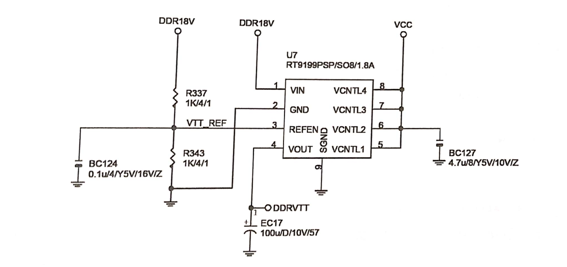
The working circuit of the memory load power supply chip RT9199 is shown in figure 3.

Figure 3 the working circuit of the memory load power supply chip RT9199.
VCC power the chip 5, 6, 7, 8 pin, DDR18V to the chip I pin power supply, DDR18V through the resistance R337 and R343 partial voltage, to obtain the voltage value of DDR18V half the VTT_REF voltage, to the chip 3 pin to provide a reference voltage input. The chip outputs from 4-pin DDRVTT power supply, the voltage value is consistent with the 3-pin reference voltage.
This article is from Allicdata Electronics Limited. Reprinted must indicate the source

