How the AMD A75 chipset motherboard works?
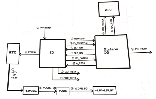
The AMD A75 chipset motherboard works as shown in figure 1.

Figure 1 schematic diagram of the AMD A75 chipset motherboard.
The AMDA75 chipset motherboard works as follows.
(1)The IO chip sends a RSMRST signal to the bridge to indicate standby power is good.
(2)The short switch generates a PWRBTN# trigger signal to the IO chip.
(3)The IO chip outputs the IO_PWRBTN# signal to the bridge request to power up.
(4)The bridge outputs a high-level SLP_S4# signal to the 1O chip to indicate that it enters the S3 state.
(5)The bridge outputs the SLP_S3# signal to the 10 chip, indicating that the power is allowed to be powered on, enters the S0 state.
(6)The 1O chip converts the PSON# continuous low level signal to the ATX power supply.
(7)The power supply green cable is low output + 12V, + 5V, + 3.3V main power supply, + 1.5VDUAL memory power supply through circuit step-down.
(8)The VCORE _ EN signal is sent to the power management chip through circuit conversion of the memory power supply.
(9)Power management chip operation control circuit output CPU power supply VCORE, voltage stable output VCORE_PG high level. VCORE_PG control voltage conversion circuit generates bridge power supply and bus power supply.
(10)The IO chip sends a SB_PWRGD signal to the bridge to indicate that the power supply is normal.
(11)The bridge sends an APU_PWROK signal to the APU, to indicate that the motherboard is powered properly.
(12)The bridge sends out a A_RST# signal to reset the IO chip.
(13)IO chip conversion output PCIE_RST#, LAN _ RST# reset PCL-E slot and Nic chip.
(14)Bridge generates PCI RST# signal reset PCI slot.
(15)The bridge sends a APU_RST# signal to reset the APU, APU power supply, clock signal, PG signal, reset signal and start working.
This article is from Allicdata Electronics Limited. Reprinted need to indicate the source.

