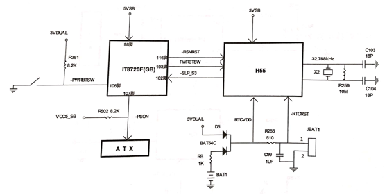
The operating principle of Intel single-bridge H55 chipset motherboard boot circuit.
The Intel Motherboard 5 Series chipset renamed the integration of the South Bridge chip and the North Bridge chip to PCH (platform Control Center). The H5SS chipset motherboard boot circuit is composed of IO chip, H55 bridge chip, RTC circuit, switch pin, ATX power interface, as shown in figure 1.

Figure 1 Operating principle block diagram of the Intel H55 chipset motherboard boot circuit.
The basic principle of Intel single-bridge H55 chipset motherboard is basically the same as that of Intel dual-bridge motherboard. The motherboard boot function is completed with the assistance of IO chip and bridge.
The first stage: the main board is equipped with CMOS battery, the battery positive through the resistance RB and diode D5 to generate RTCVDD to the bridge internal real-time clock circuit power supply, and the resistance R255 and capacitance C99 delay to get-RTCRST real-time clock reset signal to the bridge. The bridge supplies power to the crystal vibration, and the product vibration starts to produce the 32.768kHz frequency feed bridge. The real-time clock circuit inside the bridge begins to work and is used to save the CMOS settings.
The second stage: plug in the ATX power supply and connect the 220V AC power. The ATX power supply output 5VSB standby power supply directly to the 98 pins of the 10O chip IT8720F to power the IT8720F. The 5VSB is converted into 3VSB to provide standby power to the bridge. After the IT8720F chip is powered by 5VSB, it sends out-RSMRST high-level signal to the bridge through the internal delay, indicating that the standby voltage is normal, and the standby circuit is finished.
The third stage: the short switch generates the-PWIRBTSW trigger signal to the 106th pin of the IT8720F, and outputs the 3.3V-0V-3.3V jumping signal PWRBTSW from the 103pin through the internal logic conversion to the bridge request to power on. When the bridge receives a PWRBTSW signal and its standby condition is normal, the internal logic conversion outputs a 3.3V-SLP_S3 signal, which is sent to the 102nd pin of the IT8720F to indicate that power is allowed. When the-SLP_S3 signal is received by the IT8720F, the power-up is completed by internal logical conversion from the 107th pin output-PSON continuous low level pull low green wire.
This article is from Allicdata Electronics Limited. Reprinted need to indicate the source.

