How to design the simulation of piezoresistive pressure sensor?
Designing MEMS devices such as piezoresistive pressure sensors is a very challenging task, because accurate description of the working conditions of such devices requires coupling analysis based on multiple physical fields. With COMSOL Multiphysics®, you can easily couple multi-physics simulations to easily test device performance and obtain accurate analysis results. Today, we will demonstrate this powerful function of the software through an example.
Advantages of piezoresistive pressure sensors
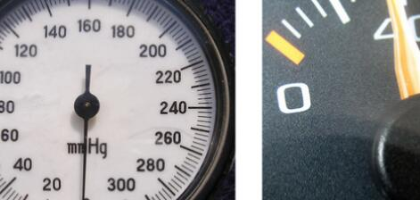
The piezoresistive pressure sensor is the first commercially available MEMS device. As the product with the highest market share of pressure sensors, this type of equipment has a wide range of uses in many applications. The most common application examples are blood pressure measuring instruments and oil (gas) meters in automobile engines.

The application of piezoresistive pressure sensors in the biomedical field and the automotive industry. Left: Blood pressure measuring device. Image taken by Andrew Butko. Licensed by CC BY-SA 3.0 and shared via Wikimedia Commons. Right picture: car fuel gauge. Image taken by Marcus Yeagley. Licensed by CC BY-SA 2.0, shared via Flickr CreaTIve Commons.
Compared with capacitive pressure sensors, piezoresistive pressure sensors have higher power consumption and relatively higher noise, but they have many advantages that capacitive pressure sensors do not have. For example, piezoresistive pressure sensors can be more easily integrated with Integration of electronic equipment. Not only that, its response to pressure is more linear, and it can also shield RF noise.
Piezoresistive pressure sensors, like other MEMS devices, also include multiple physics in their design. In order to accurately evaluate sensor performance, reliable tools are needed to couple different physical fields and describe their interactions. The rich features and functions of COMSOL MulTIphysics can definitely meet your needs. Accurate simulation results allow you to accurately understand the performance of the equipment before actual manufacturing.
We have selected an example from the "Case Download" to give you a deeper understanding of the powerful features of the COMSOL software.
Evaluate the performance of piezoresistive pressure sensors with COMSOL MulTIphysics®
The design of the "piezoresistive pressure sensor, shell" teaching model is based on a pressure sensor manufactured by the original Motorola Semiconductor Division, which later developed into Freescale Semiconductor. This type of sensor is no longer in production. Reference 1 at the end of the article provides a detailed analysis of the sensor, and Reference 2 provides the manufacturer's archived data sheet.
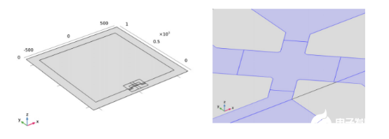
The geometry of the model consists of a square diaphragm with a thickness of 20 µm and a side length of 1 mm. Around the diaphragm is a support area with a width of 0.1 mm, which is fixed on the underside of the diaphragm and connected to the thick handle of the semiconductor material in the device. Near the edge of the diaphragm, you can see an X-shaped varistor Xducer™ (hereinafter referred to as X) and the wire connected to it. Only a small number of interconnecting wires are added in this area, and the conductivity of these connecting wires is high enough that it will not affect the output of the device.

The geometry of the sensor model (left) and the detailed view of the varistor geometry (right).
If we apply a voltage to the arm along the [100] direction in X, current will flow along the arm. When pressure causes the diaphragm of the implanted sensor to deform, shear stress is generated in the device. Due to the shear stress, an electric field or potential gradient perpendicular to the direction of the current will be generated in the arm along the [010] direction in X-this is caused by the piezoresistive effect. The potential gradients over the width of the transducer are gradually added, and finally a voltage difference is generated between the two ends of the arm of X.
In this case, we assume that the varistor has a thickness of 400 nm and a uniform p-type semiconductor with a density of 1.31×1019 cm-3. Since the connecting wires have the same thickness, we assume that the doping density is 1.45×1020 cm-3.
For the direction, the edge of the semiconductor material must be aligned with the x-axis, y-axis of the model and the direction of silicon. At the same time, the varistor forms a 45º angle with the edge of the material, that is, it is located in the direction of the crystal. In order to determine the crystal orientation, the coordinate system of the model can be rotated 45º about the z axis. With the help of the rotating coordinate system feature in the COMSOL software, we can easily complete the above operations.
In this case, we use the piezoresistive effect, boundary current interface to simulate the structural equation and the electrical equation on the thin layer, which coincides with the boundary on the structure. Using this type of two-dimensional "shell" formula can greatly reduce the computational resources occupied by simulating thin-layer structures. Please note that we have selected both "MEMS Module" and "Structural Mechanics Module" to perform the analysis.
Comparison of results
First, let us observe the displacement of the diaphragm after applying a pressure of 100 kPa.
When taking a more accurate shear stress value at the midpoint of the diaphragm edge in the local coordinate system, Reference 1 indicates that the local shear stress is 35 MPa. This result is very consistent with the minimum value of 38 MPa in the simulation study in this paper. Theoretically, the shear stress at the midpoint of the diaphragm edge should be the largest.
In view of the equipment size and the estimated value of doping degree, under normal operation, the model output is very consistent with the information in the manufacturer's data sheet. For example, in this model, an operating current of 5.9 mA can be obtained after applying a bias of 3 V. A similar 6 mA current is recorded in the data sheet. In addition, the voltage output of this model is 54 mV. As shown in the data sheet, the actual potential difference generated by the device is 60 mV.
Finally, let us look at the current and voltage distribution details of the Xducer™ sensor. Reference 3 mentioned that when the local width of the current-carrying silicon line in the voltage sensing element increases, a "short-circuit effect" may occur. The essential reason for this effect is that the current diffuses into the sensing arm of the X-shaped varistor.
This article is from Allicdata Electronics Limited which offer electronic components, semiconductors, antennas, capacitors, connectors, diodes, transistors, IC,resistors. For more product information, please go to the website to get it.

