What is the signal path from the sensor to the processor?
The factors that ultimately affect the integrity of any sensor reading begin with the three main functional blocks of the signal chain shown in Figure 1. These function blocks are:
1. Sensor and its lead
2. The analog front end in the signal conditioning IC, centered on the analog-to-digital converter (ADC)
3. Digital I / O connected to the system processor

Figure 1: The basic signal path from sensor to processor contains in principle only some basic functions, but the practical interface IC provides many additional functions and features. (Source: Digi-Key Electronics)
In a multi-channel system, various types of sensors are commonly mixed, such as thermocouples, resistance temperature detectors (RTD), and pressure sensors. Of course, the sensor may fail, or its interconnect leads may form an open circuit, or short circuit with adjacent leads, power rails, or ground.
Depending on the type of sensor, the failure of its lead may immediately appear as a "off-scale" reading. Conversely, certain failure modes can lead to inaccurate but reasonable signals. In addition, some sensors (such as RTD) require an external excitation current, and this current must be within the set range to provide a valid reading. For these reasons, it is advisable to test the continuity of the signal path between the sensor and the analog front end and check whether the signal remains between the minimum and maximum allowable limits, but it is best to use an analog that is not affected by potential problems with the ADC Circuit.
This not only provides accurate readings, but also allows the system decision algorithm to use highly reliable source data based on these readings at runtime.
However, all these additional checks and balances will add additional components, requiring a larger footprint and additional design time.
Self-interrogating IC ensures the integrity of sensor data
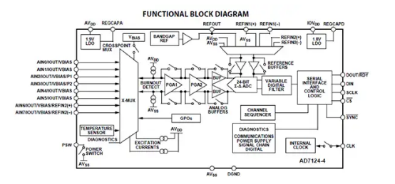
In order to meet the demand for high integrity data and at the same time have minimal impact on design time and footprint, Analog Devices has introduced the AD7124-8BCPZ-RL7, which is a sensor-centric ADC and interface whose functions go far beyond Basic signal conditioning and conversion. The product includes multiple signals and self-diagnostic functions to ensure data integrity.

Figure 2: The AD7124 is a sensor-centric ADC and interface. Its functions far exceed basic signal conditioning and conversion, including multiple signals and self-diagnostic functions to ensure data integrity. (Source: Analog Devices)
The AD7124 is a four-channel, low noise, low power, 24-bit, delta-sigma (Σ-Δ) type device. The sampling rate ranges from slightly higher than 1 sample per second (sufficient for many sensors and their applications) to 19,200 samples per second. At the lowest sampling rate, the device consumes 255 microamps (μA). Because of its design emphasis on low noise (less than 25 nanovolts (nV) rms) and low drift of the internal voltage reference (10 ppm / ° C), the reading accuracy of the device has been improved.
The AD7124 itself is packaged in 32-lead LFCSP and 24-lead TSSOP. Its flexible digital I / O supports 3-wire and 4-wire SPI, QSPI, MICROWIRETM and DSP compatible interfaces.
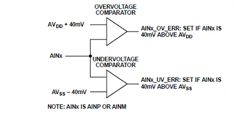
The AD7124 uses two techniques to solve the aforementioned sensor lead problems: signal limit alarm and burnout current test. The signal limit alarm uses an overvoltage / undervoltage alarm monitor to check the absolute voltage of each of the four pairs of analog input connections (Figure 3). The voltage must be within the specified range to meet the specifications in the specifications.

Figure 3: For basic verification of sensor leads using signal limit alarms, a hardware-based comparator with fixed minimum / maximum values can be used. (Source: Analog Devices)
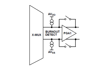
The burnout current test uses a pair of complementary programmable current sinks and current sources. By sinking a predefined pair of currents in the sensor leads, the AD7124 can verify its integrity (Figure 4). The fully open or fully closed current will be converted to the selected analog input pair to be tested.

Figure 4: By sinking a pair of predefined currents in the sensor leads, the AD7124 can verify its integrity. (Source: Analog Devices)
A full-scale reading (or near value) may mean that the front-end sensor is open. If the measured voltage is 0 volts, it may indicate that the sensor is shorted. The corresponding flag bit will be set in the error register to indicate the occurrence and type of error.
Finally, for applications where the user provides an external reference instead of using an internal reference (usually done with RTD or strain gauges), the AD7124 checks whether all external conversion reference voltages are correct.
If you want to know more, our website has product specifications for sensor, you can go to ALLICDATA ELECTRONICS LIMITED to get more information

