How does the D trigger circuit change to SR type, JK type and T type?
A basic unit circuit capable of storing a 1-bit binary signal is collectively referred to as a flip-flop (Filp-Flop)
A flip-flop is the basic logical component that makes up a sequential logic circuit. It has two stable states: "0" and "1". In different input situations, it can be set to 0 state or 1 state. When the input signal disappears, the set state can remain unchanged. So the trigger can remember a 1-bit binary signal. Depending on the logic function, flip-flops can be divided into SR flip-flops, D flip-flops, JK flip-flops, T and T' flip-flops. According to the different structural forms, basic SR flip-flops, synchronous flip-flops, master-slave flip-flops and edge triggers can be divided.
a. When the trigger is in the 1 state, ie Q = 1, if S'R' = 01 or 11, the trigger is still in the 1 state. If S'R' = 10, the flip-flop turns to the 0 state.
b. When the trigger is in the 0 state, that is, Q = 0, if S'R' = 10 or 11, the trigger is still in the 0 state. If S'R' = 01, the flip-flop turns to the 1 state.
The constraint is that S'R' cannot be 0 at the same time.
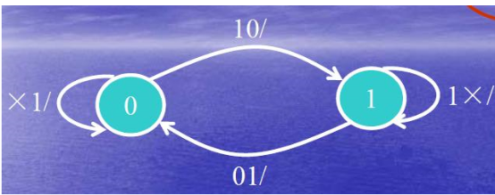
How do D flip-flops turn into SR, JK and T?
Convert D to JK trigger
By using the D-to-JK conversion table, a given D flip-flop can be converted to a JK flip-flop, as shown in Figure 1. The table collectively represents the truth table of the JK flip-flop and the stimulus table of the D flip-flop.
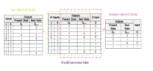
Figure1 : D-to-JK conversion table.
After that, we need to simplify the expression of the D input according to J, K and Q n . We will use K-map technology again.
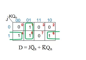
Figure 2: K-map simplification of D input based on J, K and Q n
Figure 2 shows that in order to convert a D flip-flop to a JK flip-flop, its D input needs to be driven by the output of a dual-input OR gate whose input is
Negative Ñ between the Ĵ phase and the present-state Q (ie Q Ñ)
The negation of K(K̅) is related to the current state Q n
This shows that we need
A NOT gate - a negative K.
Two with the door, one gets JQ n and the other gets KQ n
An OR gate to obtain the d input given by JQ K + KQ Ñ
Therefore, the resulting system is as shown in FIG. 3.
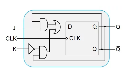
Figure 3: D flip-flop designed to be used as a JK flip-flop
Finally, verify that the designed system uses the D-to-JK verification table as expected, as shown in Figure 4.
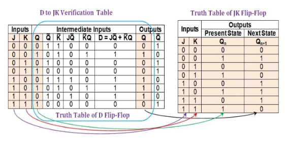
Figure 4: Comparison between the D-to-JK validation table and the truth table of the JK trigger logic.
Figure 8 shows the first, second, third and ninth columns of the D-to-JK validation table (shown in beige shades) with the same entries as the entries in the columns of the JK trigger truth table. This indicates that a given D flip-flop behaves exactly the same for each input combination and current state as the JK trigger.
Therefore, we can conclude that the conversion process is successful.
Convert D to SR trigger
The process of converting a given D flip-flop to an SR type is initiated by obtaining a table representing the information present in the truth table of the SR flip-flop and the information conveyed by the D-stimulus table. Such a table is called a D-to-SR conversion table, as shown in Figure 5.
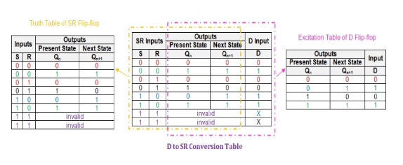
Figure 5: D-to-SR conversion table.
Note here that the last two rows of the conversion table have X (Do not Cares) in the "D Input" column. This is because when using an SR flip-flop, the input combination of S = R = 1 is invalid (because the output will be unpredictable).
The next step is to obtain a logical expression for the given D flip-flop input based on the inputs of the required flip-flops S and R and the current state Q n . However, in doing so, we need to simplify Boolean expressions as much as possible using appropriate simplification techniques (such as K-map ICfans). Here is a detailed description of Carnot's method timing.
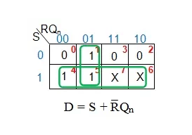
Figure 6: K-map simplification of the D input
From Figure 6, the simplified logical expression for the d input is found to be S + RQ Ñ. This means that in order for a given D flip-flop to behave like a desired SR trigger, we need AND Q n to negate the user-defined input R and then OR the result with the user-defined input.
Therefore, the additional combined circuit required will be a NOT gate, an AND gate and an OR gate. The final system designed using these components is shown in Figure 7.
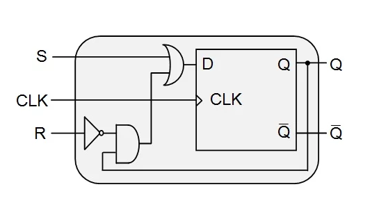
Figure 7: D flip-flops behave as SR flip-flops
After completing the conversion process, we need to continue the verification process. Here, we need to write a truth table for the designed system and compare its entries to the entries in the truth table of the SR (required) trigger.
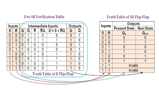
Figure 8: Comparison between the D-to-SR verification table and the truth table of the SR trigger.
The figure shows that all entries in the first, second, third and eighth columns (shown in beige shades) of the D-to-SR verification table are consistent with the entries present in the truth table of the SR flip-flop. The last two lines look different, but they can be considered equivalent because the output of the SR trigger may be high or low due to invalid input combinations. In fact, we have designed a system that is better than SR flip-flops because it has predictable output behavior when both inputs are high.
The validation table indicates that the conversion process was successful: a given D flip-flop is functionally equivalent to the required SR trigger clock.
D conversion to T trigger
In order to convert a given D flip-flop to a T-shape, we need to obtain the corresponding conversion table, as shown in Figure 9. Here, the information in the excitation table of the D flip-flop is inserted as part of the truth table of the T flip-flop.
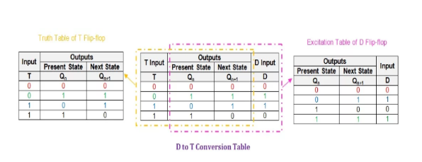
Figure 9: D-to-T conversion table.
In the conversion table obtained, the next step is to express the input, d, the terminology in T and Q.
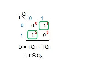
Figure 10: K-map simplification of D, expressed as T and Q n
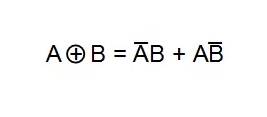
As can be seen from Figure 10, in order to convert a given D flip-flop to a T-type, we need to drive its input pin (D) through the output of the XOR gate input to T and Q n . This will result in a new digital system as shown in Figure 11(a) (semiconductor community).
If you must limit yourself to the NOT, OR and AND gates, we will need to follow these steps:
Use the AND gate to AND the user-defined input T, and the negation of the current state of the trigger Q n .
Use another AND gate to trigger the current state of the trigger and cancel T (obtained as the output of the NOT gate).
Or use a two-input OR gate to connect the outputs of the two AND gates together.
This results in the digital system shown in Figure 11(b).
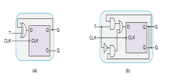
Figure 11: D flip-flop designed to use (a) XOR gates and (b) T flip-flops with only NOT, OR and AND gates.
The next and final step is to verify the conversion process using the D-to-T verification table, as shown in Figure 12.
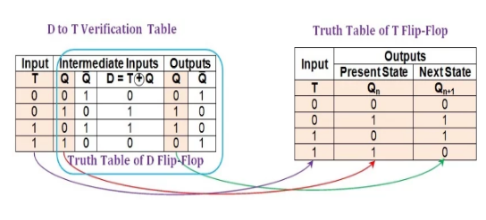
Figure 12: Comparison between the D-to-T verification table and the truth table of the T flip-flop.
As can be seen from the figure, the first, second and penultimate columns of the D-to-T verification table (shaded in beige) are identical to the columns in the truth table of the T flip-flop. This indicates that the conversion process is successful, that is, the behavior of a given D flip-flop is exactly the same as that of the T flip-flop.
Although we have verified the system designed in Figure 11(a), the conclusion is also valid for the design shown in Figure 11(b) because
If you want to know more, our website has product specifications for the triggers, you can go to ALLICDATA ELECTRONICS LIMITED to get more information

