Samsung Planning to Introduce 3nm Full-gate Transistors in 2021
Samsung Electronics plans to launch its successor to the FinFETS transistor architecture in 2021, using a gate-all-around (GAA) at the 3-nm process node. The South Korean giant also reiterated on its Tuesday (May 22) annual foundry technology forum that it will begin using extreme ultraviolet (EUV) lithography to begin 7nm production in the second half of this year.
Since the beginning of the 21st century, Samsung and other companies have been developing GAA technology. The GAA transistor is a field effect transistor (FET) with a gate on all four sides of the channel to overcome the physical scaling and performance limitations of the FinFET, including the supply voltage.
Ryan Sanghyun Lee, Samsung’s vice president of marketing, said that since 2002, Samsung’s proprietary GAA technology has been referred to as a multi-channel FET (MBCFET). According to the company, MCBFETs use nanochip devices to enhance gate control and significantly improve transistor performance.
Last year, Samsung stated that it plans to start using the 4-nm node GAA transistors by 2020. However, industry observers expect the GAA to start production by 2022.
Samuel Wang, Gartner's vice president of foundry research, said he expects Samsung to mass-produce GAA transistors at some point in 2022. "It looks like they are moving faster than this," said Wang.
Kevin Krewell said: "Samsung's road map is very radical. I already know that they are making rapid progress on EUV, but it also sets a high threshold."
However, Krewell added: "This is still a way out and the schedule may change."

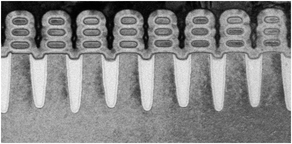
SEM images of 5nm transistors using full gate technology established by IBM and partners Samsung, Globalfoundries. Source: IBM
In June of last year, IBM and its research alliance partners Samsung and Globalfoundries described them as a stack based on the 2017 Symposia on VLSI Technology and Circuits conference in Kyoto, Japan. A process developed by nanosheets to make 5-nanometer GAA transistors. It is understood that other chip makers including Intel and TSMC are developing their own next-generation transistors, similar to FinFETs, which are GAA FETs.
Samsung reiterated plans to begin mass production using EUV lithography in the second half of this year, using the 7nm Low Power Plus process. Samsung is expected to be the first chip maker to put into commercial production EUV equipment, which has been highly expected by the industry for many years. TSMC and Globalfoundries announced that they plan to use EUV for commercial production in 2019.
Although lithography tool supplier ASML and advanced chip manufacturers have proved to be able to overcome power supply problems that have plagued EUV development for many years, support technologies needed to deploy EUV in commercial production are still being developed and adjusted.
Yongjoo Jeon, chief engineer of Samsung foundry business, said on Tuesday that Samsung will use an in-house developed EUV mask detection tool. For Samsung, this is an important advantage, because no similar commercial tools have been developed yet, Jeon added.
Jeon said that Samsung will be the first to deploy EUV without protecting the EUV mask from particle contamination masks, another technology still under development. Jeon said that Samsung is making progress in the development of EUV film, and he believes that the technology can finally be deployed in the production process of its own EUV.
Samsung is also developing EUV photoresists and is expected to achieve target mass yields for mass production later this year, Jeon said. Samsung's process technology roadmap also includes the 2019 5nm FinFET and the 2020 4nm FinFET production process.
This article is from Allicdata Electronics Limited. Reprinted need to indicate the source.

