Do you know how to design printed boards and system wiring?
When designing the printed board, the influence of the interference on the system should be taken into consideration. The analog part of the circuit and the circuit of the digital part should be strictly separated. The core circuit should be protected, the system ground should be surrounded, and the wiring should be as thick as possible. DC-DC isolation, signal isolation, design of isolated power supply, analysis of parts that are prone to interference (such as clock circuits, communication circuits, etc.) and parts that are easily interfered (such as analog sampling circuits, etc.) The circuit takes separate measures. Inhibition measures are taken for the interference components, isolation and protection measures are taken for the sensitive components, and they are spatially and electrically separated. When designing at the board level, it is also important to note that the components are placed away from the edge of the printed board, which is advantageous for shielding against air discharge.
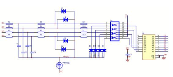
See Figure 1 for the schematic design of the sampling circuit:

Figure 1: Sampling circuit design.
The reasonable layout of the circuit can reduce interference and improve electromagnetic compatibility. According to the function of the circuit, several functional modules are divided, and the interference source and sensitive signal of each module are analyzed for special processing.
When printing printed circuit boards, you need to pay attention to the following aspects:
1, the printed circuit board width should not be abrupt, the corner should be rounded, not right angle or sharp corner.
2. Make the length of the wire as short as possible, reduce the area of the printed board, and reduce the interference on the wire.
3, try to use the chip components, the chip device is much better than the electromagnetic compatibility of the in-line device.
4, using a complete ground plane design, the use of multi-layer board design, laying the ground layer, easy to interfere with signal release.
5. Keep the electronic components away from planes that may discharge, such as chassis panels, handles, screws, etc., to keep the casing in good contact with the ground, providing a good venting channel for interference. Handling sensitive signals to reduce interference.
6. Keep the loop area to a minimum, such as the loop formed between the power supply and the ground, reduce the loop area, and reduce the induced current of electromagnetic interference on the loop. The power line is as close as possible to the ground line to reduce the difference. The ring area of the mode radiation reduces the influence of interference on the system and improves the anti-jamming performance of the system. The parallel wires are placed tightly together, and a thick wire is used for connection. The signal line is close to the ground plane to reduce interference. Add high frequency filter capacitors between the power supply and ground.
7. Ground the analog ground and the digital ground at the connection between the PCB and the outside world.
8. The high-speed logic circuit should be close to the edge of the connector. The low-speed logic circuit and memory should be placed away from the connector, and the medium-speed logic circuit should be placed between the high-speed logic circuit and the low-speed logic circuit.
9. The clock line and signal line should also be as close as possible to the ground line, and the trace should not be too long to reduce the loop area of the loop.
System wiring design
After the printed board is designed, trial production, welding debugging, system installation, considering electromagnetic compatibility design factors, cabinet structure, cable design need to pay attention to the following aspects:
1. The system sets the isolation transformer and ups to ensure that the system supplies pure power.
2. The shielded power cable is used for the main power inlet, and the magnetic ring is added. The shield is grounded 360 degrees into the cabinet.
3. Use shielded wires for the external signal lines of the system, and the ground at the entrance of the shielded cabinet is well grounded.
4. The equipment casing is close to the cabinet to avoid crossover.
5. The cabinet adopts electromagnetic shielding cabinet, which has good shielding performance, shields the system well, and reduces the influence of external electromagnetic interference on the system.
6. Strictly separate the power cable and the signal cable. The surface of the device should be in good contact with each panel and the panel. The contact resistance should be less than 0.4 ohms. The smaller the better, the better the device casing is connected to the earth. When the static electricity is released, it will not affect the normal operation of the system.
If you want to know more, our website has product specifications for printed boards and system wiring, you can go to ALLICDATA ELECTRONICS LIMITED to get more information

