Why is the two-switch forward converter considered one of the most reliable converters?
Dual-switch forward converters are widely used and are considered one of the most reliable converters. This topology is highly regarded by many design engineers for a number of reasons.
Several advantages of the converter are:
- MOSFET voltage stress is limited into the maximum supply voltage
- No dead area time requirements, no direct access opportunities
- No MOSFET body diode conduction in any case
- Ability to handle multiple isolated outputs
- No resistor and capacitor snubber circuit required
- Operational simplicity over a wide input voltage range and load conditions
Several disadvantages of the converter are:
- As a single-ended converter, it requires a larger transformer and output inductor
- Limited operating frequency due to no zero voltage switching capability (ZVS)
- requires two transistors and two fast recovery diodes
Double-switch forward converter
Dual-tube forward converter is very popular with 150W - 750W ATX power supply / silver box, it also competes with the zero voltage switch (ZVS) LLC topology. It is a hard switching topology and does not work in ZVS mode. But because of this, it offers the advantage of no body diode conduction. The input voltage of the MOSFET is the output voltage of a power factor correction (PFC) converter, and (PFC) converter is required for any power supply with an output power of ≥ 65W. The typical value of this (PFC) voltage is 380V - 400V. During turn-off, the MOSFET has an additional voltage spike from the leakage induced energy, although it is clamped by a fast recovery diode.
The basic operation is as follows: Figure 1a shows transistors Q1 and Q2, which are turned on to transfer energy from the primary side of the transformer to the secondary side. On the secondary side, the forward rectifier diode conducts energy, delivering energy to the output filter and load.
When transistors Q1 and Q2 are turned off, the transformer field current flows through the now forward biased diodes D1 and D2 and back to the power supply, as shown in Figure 1b. The two diodes continue to conduct electricity until the total excitation energy on the primary side and the energy stored in the leakage inductance are returned to the input supply. Since diodes D1 and D2 are responsible for clamping the voltage spike to the input voltage, no buffering circuitry is required. Any overshoot that exceeds the input voltage needs to be managed with a proper circuit layout to minimize stray inductance. On the secondary side, the freewheeling diode is electrically conductive and delivers the output inductor energy to the load.
Transformer reset achieved when the ON time is shorter than the OFF time (duty cycle is less than 50%) during the off-period of the primary side. In other words, the primary winding itself acts as a reset winding. The OFF time will be longer than the ON time and the transformer will be reset.
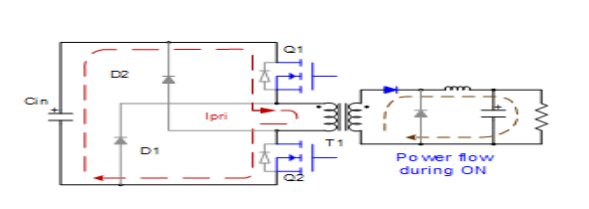
Figure 1a: Energy transfer stage of operation

Figure 1b: Power flows from the output capacitor to the electrical load
Comparison of dual-tube forward converter and PFC converter, FOM and power loss
Figure 2 compares the power loss of a two-switch forward converter with a PFC front-end converter at 400W. The MOSFET in the two-switch forward converter carries half the current and it is switched at twice the frequency (usually 125 kHz vs. 65 kHz). As this frequency doubles, switching losses become a more important factor in overall quality factor (FOM) and power loss measurements.
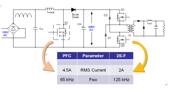
Figure 2: PFC converter vs. two-switch forward converter
To further illustrate, consider a TO-220 / TO-220F device with a maximum power loss of 8W. Suppose this is the best choice for PFC applications. The optimum meaning is that the conduction loss is 40% - 50% of the total loss at rated power. Is this also the optimal solution for a two-switch converter? The answer is of course not. In a two-switch topology, Coss/Qoss and Qsw contribute approximately 87% of the total loss, with the remainder being conduction losses. This imbalance between conduction losses and switching losses is very detrimental to efficiency and cost. The reason why the conduction loss is smaller than that of the single-switch PFC converter is that each MOSFET used has half the current of the single-switch PFC circuit while switching at twice the frequency at the same time.
Any switching circuit has two switching losses. The first type of loss due to the Vds x Ids transition that occurs during turn-on and turn-off. These losses are measured by the so-called "Qsw", which is a combination of Qgd and Qgs, representing the effective switching charge of the MOSFET. Switching losses are a function of load and switching frequency.
The second type of switching loss is related to the charge and discharge of the MOSFET output capacitance Coss. In ATX power supplies, the popular two-switch forward converter is followed by an input voltage of approximately 400V. Therefore,the output capacitor Cos switching loss is a large part of the total loss. The device's Coss / Qoss is a very important loss, especially at light loads, the switching losses exceed the conduction losses.This loss is essentially independent of the load and Qsw and needs to be considered along with Qsw when choosing the right MOSFET. The loss-based FOM associated with a particular application is:

The Coss of the high voltage MOSFET varies considerably depending on the applied VDS. To illustrate the nonlinearity of the output capacitor, available Poss = ½ Co (er) x V2 x Fsw as an approximation of loss formula. (Co(er) is the equivalent capacitance, which has the same loss as Coss, and usually Coss is included in the specification). It should be noted that the loss associated with the output capacitor (an important part of the total loss formula in any high-voltage topology) is not considered in the industry standard FOM=RDS(on)(typ)x Qg(typ) . However, they are essential for the application-specific FOM (for device selection) used in this analysis.
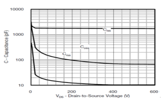
Figure 3b: Planar technology capacitance curve
With this requirement in mind, we present a list of components that we believe will achieve the highest efficiency of a two-switch forward converter under typical operating conditions to ensure the most efficient design. Each MOSFET has a target loss of less than 0.5% of the total converter losses. Therefore, for a 400W ATX power supply, the loss will not exceed 2W per device. Table 1 illustrates the assumed operating conditions for such power supplies.
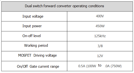
Table 1: Design conditions for dual-switch forward converter
“X” is the model number that represents the package. For the same electrical feature set, there are a number of package options to choose from. The package used will depend on the power stage and what kind of package MOSFET is actually allowed.
Figure 4 defines the package, current rating, voltage, and device technology for different product codes [1].
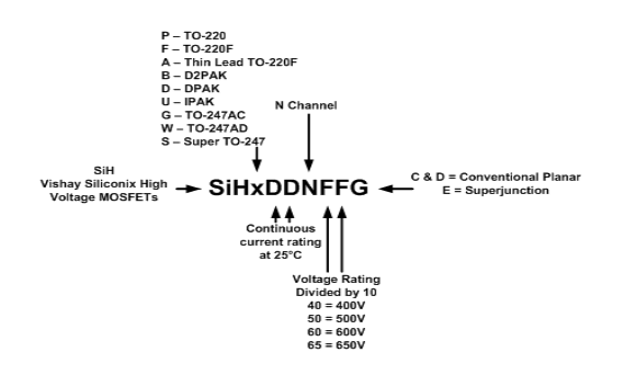
Figure 4: Product Code Definition
Table 2 lists the recommended maximum power ratings for products in different packages due to the many package options available.
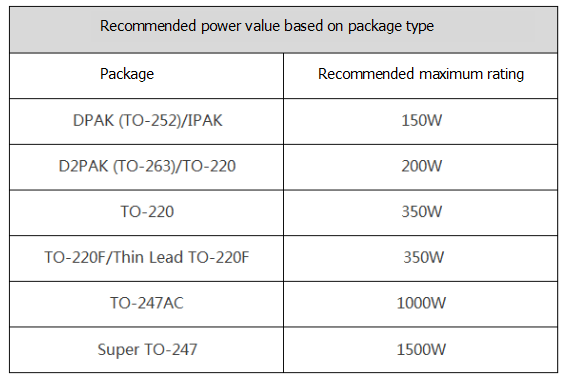
Table 2: Maximum power value based on package type
Table 3 shows the corresponding devices for different power values, including design conditions, device code understanding, and maximum recommended values based on the package.
This table lists many different devices. Depending on whether we are more concerned with voltage, efficiency or price, we can choose the device that best suits your application.
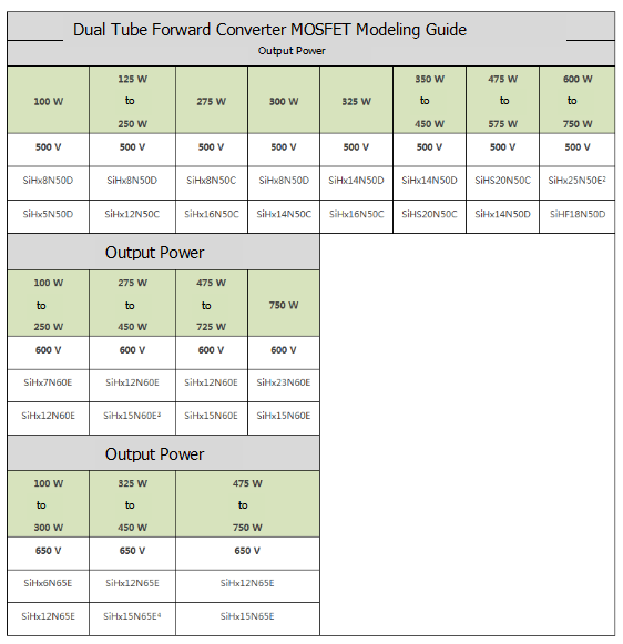
Table 3: Device Selection Tool Based on PFC Output Power Value
Note: Devices with "x" are available in a variety of packages; 500V devices use traditional planar technology, while 600V and 650V provide superjunction technology.
If you want to know more, our website has product specifications for converters, you can go to ALLICDATA ELECTRONICS LIMITED to get more information

