Intel single bridge H55 chipset motherboard timing.
The timing analysis of GA-H55M-S2H motherboard is as follows.
1. Install the battery BAT, battery positive electrode through the resistance RB changed its name to VBAT, all the way to the IO chip to measure the battery power, the other way to the Schottky diode D5 1 pin, output RTCVDD from 3 pin to power the bridge RTC circuit, As shown in figure 1. RTCVDD through the delay circuit composed of R255and C99, the delay obtains-RTCRST high level, sends to the bridge RTCRST# pin, resets the real-time clock circuit.

Fig. 1 RTCVDD and-RTCRST generation circuits.
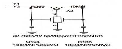
2. South Bridge chip supplies power to X2 crystal oscillator, which produces 32.768kHz frequency to provide reference frequency for RTC circuit inside the bridge, so that RTC circuit can save CMOS settings, such as time, date and so on, as shown in figure 2.

Fig.2 32.768kHz crystal oscillator
3. Plug in the power supply to output the SVSB voltage, change the name to the IT _ VCCH through R472, and provide standby power to the IO-chip, as shown in Figure 3.

Figure 3IT _ VCCH conversion circuit
4. The other 5 VSB standby power supply is stepped down through the regulator Q40 to obtain a 3.3 V 3 VDU AL _ ICH standby voltage, as shown in Figure 4.

Figure 4 3 VDU AL _ SB Voltage Conversion Circuit.
The 3VDUAL _ ICH voltage is filtered by the capacitors BC150, BC148, BC120 and sent to the bridge VCCSUS3 3 pin to provide standby power to the bridge, as shown in Figure 5.

Figure 5. Bridge chip standby power supply circuit.
5.IO After the standby power supply of the chip TT8720F is normal, the-RSMRST signal of high level is output from 116 pin. As shown in FIG.6, the circuit shown in FIG.7 is pulled to a high level of 3.3 V, and is sent to the bridge to indicate that the standby power supply of the main board is normal.

Fig. 6 IO the chip sends out the H-RSMST circuit.

Figure 7-RSMRST pull-up circuit.
3VDUAL_ICH standby power supply is pulled up to 3.3 V voltage by resistance R4, and then filtered and delayed by capacitor CIO0, as shown in figure 8.
6. The 6 pin and 8 pin of the short front panel switch lead to the 3.3V-0V33V jump-PWRBT_1 trigger signal, which is renamed PWRBTSW through the resistance R380 (see figure 9) and sent to the 106 pin of the IO chip IT8720F (see figure IO).

Fig. 9 switch needle arrangement circuit.
After the internal logic conversion of the IO chip IT8720F, the PWRBTSW signal is sent out from the 103 pin (see figure IO). The 3.3V-0V-3.3V jump signal is the same as the-PWRBTSW signal, and the PWRBTN# pin sent to the bridge is powered on.

Fig. 10 IO chip trigger signal.
The bridge receives the PWRBTSW power-on request signal, and the output lasts 3.3 V after the well and bridge standby condition and the body are normal. High-S4 _ S5 and-SLP _ S3 signals, as shown in Figure 9.

FIG.9 is a south bridge chip output signal.
And the S4 _ S5 signal is converted into an EN signal to control the power supply management chip to work and output the memory for power supply through the new circuit of FIG.10i

Figure 10 S4 _ S5 Conversion Circuit.
The operation principle of the circuit shown in FIG.10S4 S5 turns on the Q65 through the resistor R458, and the Q69 is turned off, and the EN signal is controlled to a high level through the inside of the ISL6545 chip, and the operation of the chip is started to control the output memory to supply power.
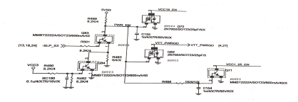
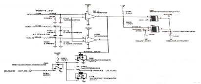
The path of the -SLP S3 is returned to the IO2 pin of the IO chip IT8720F, indicating that power-on is allowed, as shown in FIG.8, the two paths are converted to the VCC18 EN signal through the circuit as shown in FIG.11, and the three-way control circuit converts the circuit conversion output 5 VDU to be supplied with two-way power supply.

Figure 11 VCCI8EN conversion circuit.

Fig. 12 5VDUAL conversion circuit.
9.The trigger signal of 3.3V-0V-3.3V jump is obtained by IO chip 106 after the high level of 3.3V is obtained, the continuous low level-PSON signal is outputted from 107 pin to 16 pin of ATX power interface after logic conversion in the internal circuit of the chip. Pull down the green line of the power supply, so that the power output of each main power supply to complete the power, as shown in figure 13. 107

Fig. 13 ATX power interface circuit.
IO. After the power supply outputs each main power supply, the VCC18_EN controls the circuit shown in Fig. 10-37, and the VCC3 is stepped down to get the power supply of the VCC1_8_PCH bridge.
The 2_5LEVEL voltage of 2.5V is 1.83 V through the resistance R46 and R52 partial voltage, and the VCC18_EN is pulled back to the IO pin of the operational amplifier UIOC. The IO-pin voltage of the operational amplifier is higher than that of the 9-pin voltage, and the 8-pin output high level is sent to the 1-pin of Q21 by R198 current limit. The VCC1_8_PCH bridge power supply voltage of 1.83V is obtained by controlling Q21 to reduce the voltage of VCC3.

Figure 15. The VCCI 8 PCH Power Supply Generation Circuit.
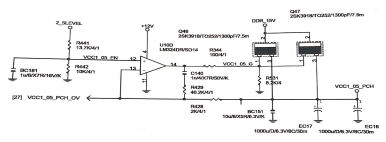
11. The internal power supply of the DDR 15 V is reduced by the circuit shown in FIG.16 to obtain the power of the VCC1 _ 05 _ PCH bridge of 1.05 V.

Figure 16. VCCI 05 PCH Bridge Power Generation Circuit.
12. VCC is controlled and reduced by the ISL6322 chip to obtain a bus power supply CPU VTT, the bus power is supplied to 33 pin of the ISL6334 of the power management chip through the VTT PWRGD signal which generates a high level by the circuit shown in FIG.17, and the operation control output CPU of the power management chip is turned on to supply the VCORE voltage.

Figure 17 VTT PWRGD generation circuit.
Figure 17 shows how the circuit works: the 2 SLEVEL voltage of 2.5 V is 0.5 V voltage through the resistance R47 and R437 partial voltage, which is sent to the 6 pin of UIOB. When the 1.2V bus power CPU VTT is normal, it is sent to the 5 pin of UIOB through the electric positive R 459. At this time, the 5-pin voltage of UIOB is higher than the 6-pin voltage, the 7-pin output 12V high level, and the 1.532V voltage is obtained by resistance R436 and R477 partial voltage, and the VTT PWRGD signal is pulled up and output.
13.After the CPU power supply VCORE voltage is stabilized, the power management chip ISL6334 outputs the high level power supply good signal VR RDY, through the R211 to the transistor Q32 B pole, causes the Q32 conduction, the Q33 cutoff, through the R244pull to obtain the 3.3V high level PCH VRMPWRGD signal, As shown in figure 18. All the way to the VTT PWRGD pin of the clock chip, turn on the clock chip to work, output each clock signal to provide the working clock to each component of the motherboard. The other way to the bridge's SYS PWROK pin (see figure 19) indicates that the power management chip is working properly.

Figure 18 PCH VRMPWRGD conversion process.

Fig. 19 SYS PWROK signal reception for bridge.
14.After the ATX power supply voltage is stable, the 5V high level and the 513V PWOK0N (see figure 20) are outputted from the 8 pin to give the good signal to the bridge source PWOK.. The 128 pin 177, which reach 187207, are internally converted from the 63PWROK pin, indicating that the power supply voltage is normal.

Figure 20 IT8720F outputs PPWROKI signal.
15. After the bridge gets the bridge power supply, the clock signal, and receives the SYSPWROK and PWROK signal, sends the DRAM PWROK to the CPU to indicate the memory power supply is normal, and then sends the CPUPWROK signal to the CPU, as shown in figure 21, indicating that the motherboard power supply is normal.

Figure 21 CPU receives a good power supply signal.
16. The bridge PLTRST# pin outputs the reset signal of the platform, and changes its name to-PFMRST to the 8-pin reset IT8720F chip sent to IT8720F by resistance over R249 (see figure 20).
17.The IO chip IT8720F emits from 65 pin-PFMRST1, is converted to-CPURST reset CPU. via the circuit shown in figure 22 .

Fig. 22 CPURST conversion circuit.
18.CPU power supply, clock signal, good power signal normal, after receiving the reset signal to start working.
If you want to know more, our website has product specifications for Intel single bridge H55 chipset, you can go to ALLICDATA ELECTRONICS LIMITED to get more information

