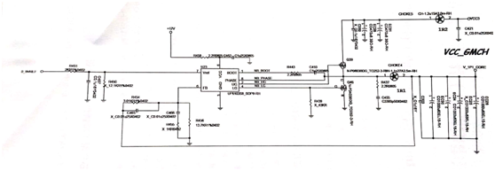
Analysis of the power supply circuit of the main board bridge of the Intel G41 chipset.
The UP6103 control is commonly used on the IntelG41 chipset motherboard to generate bridge-powered V_IPI_CORE, as shown in figure 1.
1. + 12V main power supply supplies 5-pin power to chip UP6103 through resistance R458, BOOT pin supplies power through chip interior, 0 _ 9VREF voltage passes through R451 current limit and C457 filter, and sends to chip 7 pin as opening signal.
2. The VCC3 voltage is filtered through inductors and capacitors to the D pole of the Q39.
3. UP6103 satisfies the conditions of VCC, VREF and BOOT, and outputs high level from 2-pin NB_HG to make Q39 on, and VCC3 outputs stable bridge supply V_IP1_CORE through Q39, inductive energy storage and capacitive filter.
4. The V_1P1_CORE voltage passes through the resistance R454 and R456 in series to obtain 0.9V voltage, which is fed back to the 6-pin of the chip.
5. When the output voltage is higher than 1.1V and the voltage value obtained after resistance R454 and R456 partial voltage is higher than 09V, the chip will pull down the NB_HG and close the output, and the NB_LG will be set as a high-level open lower transistor, because the current on the inductor cannot change abruptly. Then the Q46 forms a circuit to carry out the discharge and continue to provide the bridge with a working voltage.
6. When the output voltage is below 0.9V after the voltage division, the chip will turn off Q46, turn on Q39, and output power. Under the control of UP6103 chip, Q39 and Q46 cycle-on work, after capacitance, inductance filtering to provide voltage-stabilized power to the bridge.

Fig.1 V_1P1_CORE supply power generate to circuit
This article is from Allicdata Electronics Limited. Reprinted need to indicate the source.

