Analysis of the power supply circuit of the main board bridge of the RS880 chipset.
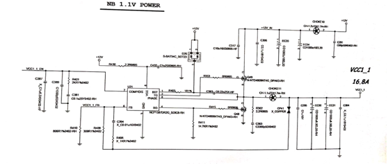
The AMD RS800 chipset motherboard commonly uses the NCP1587 chip to generate a bridge to power the VCC1_1, as shown in figure 1.
1. + 12V goes all the way through R430 to power NCP1587's 5-pin VCC and the other way through D26 to power one.
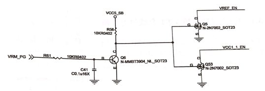
2. VCC1_1_EN is pulled to a high level through the inside of the chip 7 feet (see figure 2), the chip starts working, and the 2-pin output high level makes Q49 on.
3. + 12V charges the inductor to the capacitor through Q49 and outputs a stable VCCI_1 bridge.
4. VCC1_1 gets 0.8V voltage feedback to chip 6 after resistance R409 and R410 partial voltage. When the output voltage is higher than VCC1_ 1 and the voltage value after resistance series voltage is higher than 0.8V, the chip will turn off Q49 and turn on Q48, The electrical energy stored by inductors and capacitors supplies power to the bridge and forms a loop through Q48. When the output voltage is lower than VCC1_ 1, the chip will close the lower tube, make it cut off, turn on the upper tube, output power supply, so that cycle, stable output bridge power supply.

Fig.1 generate a bridge to power the VCC1_1

Fig.2 VCC1_1_EN switch circuit
This article is from Allicdata Electronics Limited. Reprinted need to indicate the source.

