How the Intel H61 chipset motherboard works?
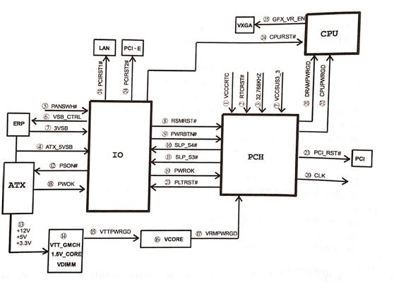
The Intel H61 chipset motherboard works as shown in figure 1.
The Intel H61 chipset motherboard works as follows.
(1) VCCRTC supplies power to the real-time clock circuit inside the bridge.
(2)RTCRST# provides reset to the internal real-time clock circuit of the bridge.
(3)Crystal oscillation provides the bridge with 32.768kHz frequencies.
(4)Plug in the power supply to output the ATX_5VSB voltage and provide 5V standby power to the IO chip.
(5)Generate high and low jump trigger signal PANSWH # to the IO chip according to the switch.
(6)The IO chip outputs the VSB-CTRL signal and sends it to the ERP energy-saving control circuit.

Figure 1 operating principle block diagram of the Intel H61 chipset motherboard.
(7)The ERP energy-saving control circuit works, outputting the 3VSB voltage, and providing 3.3V standby power to the IO chip and bridge.
(8)The IO chip outputs an RSMRST# signal to the bridge, indicating that standby power is normal.
(9)The IO chip delayed the output of the PWRBTN# signal and sent the request to the bridge to power on.
(10)The bridge outputs a continuously high-level SLP_S4# signal to the IO chip and turns on memory power.
(11)The bridge re-outputs a continuously high-level SLP_S3# signal to a IO chip to indicate that power is allowed.
(12)The IO chip sends out the PSON# continuously low level to the ATX power supply.
(13)When the green cable of the ATX power supply is pulled down, the main power supply, such as + 12V, + 5V, + 3.3V, etc., is the main power supply output of the power supply.
(14)The main power supply is depressurized by the power supply circuit, which is powered by memory, bridge and bus.
(15)Bus power supply through circuit conversion, output VTTPWRGD signal, sent to the power management chip EN pin.
(16)The power management chip works, the control circuit step down to get VCORE to power the CPU.
(17)The power management chip outputs the VRMPWRGD signal to the bridge, indicating that the CPU is powered normally.
(18) ATX power supply gray line delay output PWOK signal to IO chip.
(19)The IO chip outputs the PWROK signal to the bridge after conversion, indicating that the power supply is working properly.
(20)Bridge internal clock circuit to work, output clock signal to the motherboard equipment.
(21)The bridge sends a DRAMPWRGD signal to the CPU, to indicate that the memory is powered properly.
(22)The bridge sends an CPUPWRGD signal to the CPU, to indicate that the motherboard is powered properly.
(23)The bridge sends out a PLTRST_L signal and resets the IO chip. The IO chip generates PCIRST1# and PCIRST2# signals and resets the Nic chip and the PCI-E slot.
(24)The IO chip sends out the CPURST# signal and resets the CPU.
(25)After the motherboard runs normally, the CPU sends out a GFX_VR_EN signal to power on the video card.
Note: most H61 motherboards do not use the deep hibernation feature, so the deep hibernation circuit principle is not analyzed here. When the deep hibernation feature is not used, the bridge's deeply dormant powered VCCDSW is connected to the VCCSUS3_3 standby power supply, and the deep dormant power good signal DPWROK is connected to the RSMRST# signal.
This article is from Allicdata Electronics Limited. Reprinted must indicate the source

