The motherboard clock circuit works principle
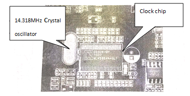
On the motherboard, all kinds of devices need to work under a unified reference clock, if the clocks of each part of the clock can not be synchronized, the various devices will not work normally, will cause a panic, work instability, or even unable to work. The clock circuit on the motherboard consists of a 14.318MHz crystal oscillator and a clock chip (see figure 1). When the working voltage of the clock chip reaches the requirement, it starts to work to supply power to the crystal oscillator. When the 14.318MHz crystal oscillator starts, it provides a reference clock frequency of the 14.318MHz for the clock chip. Then, through the conversion of the power supply circuit on the main board to the clock chip, the clock chip sends out all kinds of clock frequency required for the operation of each part of the circuit on the main board.

Fig.1 The clock circuit on the motherboard.
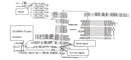
If the clock circuit on the motherboard is not working properly, it will cause a variety of different phenomenal of the failure of the motherboard. For example, CPU clock signal is abnormal, it will lead to reset no code; North Bridge chip clock signal abnormal, will lead to no CPU reset or no running code; South Bridge chip clock signal abnormal, will lead to no reset; The network card chip clock signal is not normal, will lead to unable to access the Internet. The working conditions of the clock chip are generally 3.3V main power supply, VTTPWRGD (#), 14.318MHz, and some chips also have RESET# signal (connection reset switch). The clock circuit works as shown in figure 2.

Fig.2 The clock circuit works
Main board short switch power, power output main power supply + 12V, + 5V, + 33V power supply, VCC3 voltage through resistor to the clock chip power supply. The clock chip supplies power to the crystal oscillator, and the crystal oscillator starts to produce the 14.318MHz rate to the clock chip. The RESET# is directly connected to the reset switch or VCC3 via resistor. The CK _ PWRGD high level is converted from the external circuit to turn on the clock chip to work, and the clock signal is output to the corresponding equipment on the board.
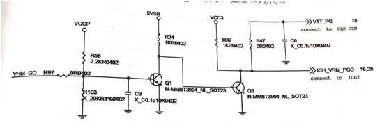
The power management chip outputs a VRM_GD high level, which is sent to the B pole of Q1 through a resistor R97 to make Q1 on and Q3 cut off, and a 3.3V high level VIT_PG signal is obtained through the R32 pull-up, as shown in figure 3.

Figure 3 VTT conversion circuit.
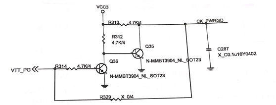
The VTT_PG is delivered to the B pole of the Q36 by the resistor R314, making the Q36 on and off the Q35, and the 3.3V high-level CK_PWRGD signal is sent to the clock chip through the resistive R313 pull-up and the clock chip is turned on, as shown in figure 4.

Figure 4 CK_PWRGD conversion circuit.
This article is from Allicdata Electronics Limited. Reprinted must indicate the source.

