Intel dual bridge G41 chipset motherboard timing.
The timing analysis of gigabyte GA-G41M-ES2L motherboard is as follows.
1.After installing the battery BAT, battery 3V voltage after the resistance RB, it is renamed VBAT, all the way to the 1O chip to measure the battery power, and the other way to the 1 pin of the Schottky diode D2. The output RTCVDD from 3 pin supplies power to the RTC circuit inside the North bridge chip. RTCVDD obtains-RTCRST high level 3V through the delay circuit composed of R183 and C124, sends to the RTCRST# pin of the North bridge chip, and resets the real-time clock circuit inside the North bridge chip. As shown in figure 1.

Fig. 1 RTCVDD and-RTCRST generation circuits.
2. The North bridge chip supplies power to the X2 crystal oscillator, which generates the 32.768H2 frequency clock signal to the ABI AB2 pin of the South bridge chip, provides the reference frequency for the internal RTC circuit of the North bridge chip, and makes the RTC circuit maintain the CMOS setting, such as time, date, etc. As shown in figure 2.

Fig. 2 32.768kHZ crystal oscillator circuit.
3. Connected to 20V electricity, ATX power output 5VSB special power supply. IT8718F 98 pin provide standby working voltage, as shown in figure 3.

Fig. 3 1O chip special machine power supply circuit.
4. The other 5VSB standby power supply is reduced by KQ1 voltage regulator to obtain 33V 3VDUAL SB standby voltage, as shown in figure 4.

Fig. 4 3VDUAL_SB voltage conversion circuit.
The 3VDUAL_SB voltage is sent to the ICH7 South Bridge chip VCCSUS3_3 pin through C96 capacitance filter to provide standby power supply to the South Bridge chip, as shown in figure 5.

Fig. 5 South Bridge chip special machine power supply circuit.
5.After the standby power supply of IO chip IT8718F is normal, the output-RSMRST signal is output from 116 pin (see figure
6. After pulling to 3.3V high level through the circuit shown in figure 7, it is sent to North bridge chip to indicate that the standby power supply on the motherboard is normal.
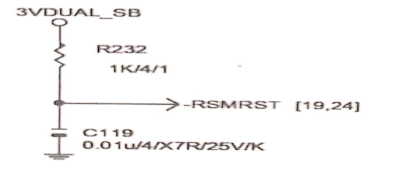
7.3VDUAL_SB standby power supply pulls up-RSMRST# to 3.3V voltage through resistance R232, and then filters and delays through capacitor C119, as shown in figure
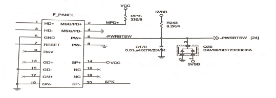
8. The 6 pin and 8 pin of the short front panel switch pin generate-PWRBTSW trigger signal, as shown in figure 8, the-PWRBTSW signal is a 3.3V-0V-3.3V jump sent to 10 chip IT8718F 106 pin (see figure 9).

Figure 6 1O chip emits-RSMRST.

Figure 7-RSMRST pull-up circuit.

Fig. 8 switch needle arrangement circuit.
9. After the internal logic conversion of the IO chip, the trigger signal sends out the PWRBTSW signal from the PWRBTSW chip (see figure 9). PWRBTSW signal, like-PWRBTSW, is the 3.3V-0V-3.3 jump signal, which is sent to the PWRBTN# pin of the ICH7 South Bridge chip to request power on.

Fig. 9 trigger signal circuit.
10.The iCH7 South Bridge chip receives the PWRTW power up request to direct, and the South Bridge chip special machine condition and the body normal uses the bridge piece to choose the continuation 3V, the electronic 945A.31 is shown in Fig. 10.

Fig. 10 South Bridge chip output signal.
11.The S4 S5 signal is converted into EN signal control memory power supply management chip through the circuit shown in Fig. 11, and the output memory power supply is output. The-SLP S 3 returns the 102 pin of the IO chip 1T8718F, as shown in figure 9), indicating that power on is allowed.

Fig. 11-S4 S5 conversion circuit.
12. -S4 S5 turns on Q22 through resistance R217, Q29 cuts off, and EN signal pulls up to a high level through the chip. The trigger signal of 3V_0V3.3V jump is obtained by IO chip 106. after the high level of 3.3V is obtained, after logic conversion in the internal circuit of the chip, the continuous low level-PSON signal is outputted from 107pin to 16 pin of ATX power interface . Pull down the power supply green line so that the power output each main power supply to complete the power, as shown in figure 12.

Figure 12 ATX power interface circuit.
13. After each main power supply is outputted, the bridge power supply is obtained by step down, and the bus power supply is obtained by depressing the circuit shown in Fig. 13.

Fig. 13 bus power supply generation circuit.
14.The 2 _ 5LEVEL voltage of 2.5V is sent to the 5 pin of the comparator U4b through the resistance R223 and R209 partial voltage, the 5 pin voltage is higher than the 6 pin voltage, the 7 pin output high level is sent to the 1 pin of Q5 through the R58 current limit, and the Q5 conduction is controlled. The power supply of VTT GMCH bus is 1.207V by depressing DDR18V and getting 1.207V power supply by VTT_GMCH bus. VTT_GMCH bus power supply through the circuit shown in figure 14, generate a high level of VTT_PWRGD signal sent to the EN pin of the power management chip, turn on the power management chip to work, control the output CPU power supply VCORE voltage.

Fig. 14 VIT_PWRGD generation circuit.
The 2.5 V 2_5LEVEL voltage is sent to the 2 pin of U4A through the resistance R 222 and R 2 7 7 partial voltage. When the 1.2V bus power supply VTT GMCH is normally sent to the 3 pin of UA, the voltage of 3 pin is higher than 2 pin. The high level of 12V output from 1 / 2 pin is 2.717V voltage through resistance R245 and R246 partial voltage, and the output is pulled up to the VTT_PWRGD.
15. When the VCORE voltage of CPU power supply is stable, the power management chip outputs a good signal of high level VR RDY power supply, which is sent to the B pole of transistor DQ11 through DRI9, so that the DQ11 is turned on, the DQ10 is cut off, and the 3.3V high level VRMGD signal is obtained by pulling up the DR46. The VTTPWRGD pin sent to the clock chip, as shown in figure 15, turns on the clock chip, outputs each clock signal, and provides the working clock for each component of the motherboard.
The ICH _ VRMGD signal of the South Bridge chip is not controlled by the power management chip, but directly pulls to the VCC3 voltage through the resistance R208 to get a high level to the South Bridge chip, as shown in figure 16.

Fig. 15 VRMGD conversion circuit.

Fig. 16 ICH_VRMGD pull-up circuit.
16.After the voltage of ATX power supply is stable, the good signal of 5V high level power supply is outputted from 8 pin. PWOK, outputs 3V PWROKI signal to ICH7 South Bridge chip and sends it to 126 pin of IT8718F. After internal conversion, IT8718F, The output of 3.3V PWROK1 signal from 63 pin to the PWROK pin of ICH7 South Bridge chip indicates that the power supply voltage is normal, as shown in figure 17.

Figure 17 1T8718F outputs PWROKI signal.
17. The south bridge chip gets the bridge power supply, the clock signal and receives the ICH VRMGD and PWROK phase and sends out CUWROK to CUP, to indicate that the motherboard power supply is normal as shown in figure 18.

Fig. 18 South Bridge chip outputs CPUPWROK signal.
18. The South Bridge chip outputs the PLTRST# reset signal (see figure 19), and the 68-pin reset IO chip IT8718 sent to the IT8718F by the resistance R146 (see figure 17). 10 the chip IT8718F outputs the PFMRST1 signal from 64 pin through internal conversion. Reset the north bridge chip to the RSTINB pin of the north bridge chip.

Fig. 19 South Bridge chip emits PWLTRST# signal.
19. The South Bridge chip emits a-PCIRST signal and resets the PCI slot, as shown in figure 20.

Fig. 20 South Bridge chip sends out-PCIRST reset signal.
20. The clock signal is normal and the clock signal is normal. After receiving the PFMRST1 reset signal sent by IO chip, the-CPURST signal is sent out through the internal delay Ims, as shown in figure 21. The G32 pin (that is, RESET pin) that is sent to the CPU socket via C36 capacitor delay is reset CPU, as shown in figure 22. CPU power supply, clock signal, CPUPWROK and-CPURST are normal, CPU starts to work.

Figure 21 North Bridge Chip Emission-CPURST.

Figure 22 CPU reception-CPURST.
If you want to know more, our website has product specifications for Intel dual bridge G41 chipset motherboard timing, you can go to ALLICDATA ELECTRONICS LIMITED to get more information

