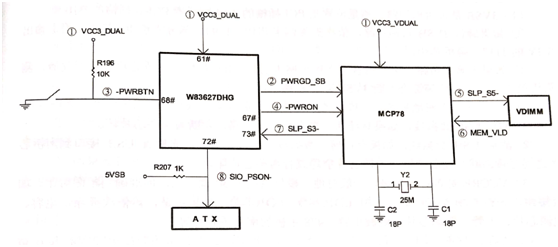
nVIDIA chipset motherboard boot circuit.
The nVIDIA chipset has two chipsets MCP68 and MCP78 in the existing maintenance, from then on slowly out of the motherboard chipset market, the commonly serviced motherboard ASUS M2N68 and M4N78 two models. The operating principle of the MCP78 chipset motherboard boot circuit is shown in figure 1.

Figure 1 nVIDIA MCP78 chipset motherboard boot circuit working block diagram.
The first stage: plug in ATX power supply, output 5VSB standby power supply, after circuit conversion to get VCC3_DUAL voltage, provide standby power to IO chip and MCP78 bridge, at the same time, pull a 3.3V high level on switch pin through resistance. After the standby voltage of the bridge is normal, it supplies power to the crystal oscillator, and the crystal oscillator produces the 25MHz frequency feed bridge. The output of the RSMRST_IO high-level signal to the bridge indicates that standby power supply is normal after the standby power supply is obtained by the IO chip.
The second stage: the short switch generates-PWRBTN trigger signal to the IO chip and 68 pins, and the IO chip converts the output-PWRON signal to the bridge request through the internal logic circuit. The bridge first sends out a 3.3V high-level SLP_S5- signal, which is sent to the memory power supply circuit to control the generation of VDIMM memory power. The memory power is then converted into a MEM-VLD high-level feed bridge to indicate that the memory is normal. The bridge then sends out a persistent high-level SLP_S3- signal to the IO chip to indicate that power is allowed. Finally, the IO chip sends out the sustained low-level SIO _ PSON signal to pull down the ATX power supply green line, and the ATX power supply outputs each main power supply to complete the power-up.
This article is from Allicdata Electronics Limited. Reprinted must indicate the source.

