What are the effects of using FPGA with on-chip high-speed network?
Since FPGAs were first introduced decades ago, each new architecture has continued to use bit-wise routing structures. Although this method has been successful, with the rise of high-speed communication standards, it is always required to continuously increase the bit width of the on-chip bus to support these new data rates. One consequence of this limitation is that designers often spend a lot of development time trying to achieve timing closure, sacrificing performance to place and route their designs.
Traditional FPGA wiring is based on multiple independent segmented interconnects (segments) running in the horizontal and vertical directions in the entire FPGA, with a switch box at the intersection of the horizontal and vertical wiring to realize the connection of the channels. Through these independent segments and switch boxes, a path from any source to any destination can be constructed on the FPGA. This unified structure of FPGA wiring provides great flexibility for realizing any logic function and can be used for any data path width in the FPGA logic array.
Although bit-wise routing in FPGAs is very flexible, the disadvantage is that each segment adds delay to any given signal path. Signals that need to be transmitted over long distances in the FPGA will cause connection delays between segments, thereby reducing the performance of the function. Another challenge of bit-wise routing is congestion, which requires the signal path to bypass congestion, which will cause more delay and cause further performance degradation.
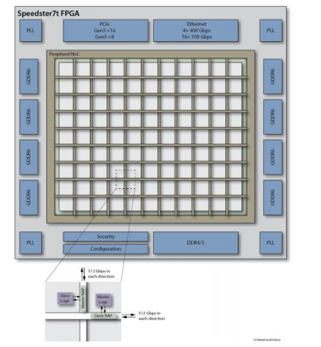
Achronix sees this challenge as an opportunity to develop a new architecture to eliminate the design challenges of traditional FPGAs and improve system performance. Achronix's solution is to build a revolutionary two-dimensional (2D) high-speed network on chip (NoC) for its brand-new Speedster7t FPGA series devices on top of the traditional segmented FPGA wiring structure. Speedster7t NoC is connected to all on-chip high-speed interfaces: 400G Ethernet, PCIe Gen5, GDDR6 and multiple ports of DDR4/5.
The inside of the NoC is composed of a set of rows and columns, which distribute the network data traffic from the horizontal and vertical directions in the entire FPGA logic array. The main NoC access (NAP) point and the secondary NoC access point are located at the intersection of each row and each column of the NoC. These NAPs can be the source or destination between the NoC and the programmable logic array.

Figure 1: Speedster7t's network on chip (NoC) and interface
Ethernet: Ethernet
Security: Security
Configuration: Configuration
each direcTIon: each direction
Speedster7t's NoC seems to only help the wiring bus inside the FPGA; however, this new architecture can significantly improve the efficiency of designers, realize new design functions, and provide the ability to easily implement intensive data processing applications. The eight application scenarios that are most significant in terms of efficiency improvement, design changes, and performance improvement are listed below.
If you want to know more, our website has product specifications for on-chip high-speed network, you can go to ALLICDATA ELECTRONICS LIMITED to get more information

