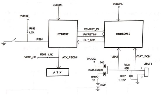
The operating principle of AMD single-bridge A55 chipset motherboard boot circuit.
A55 CPU with FMI and FM2 support The working principle of the trigger circuit is shown in figure 1.

Figure 1 Block diagram of the operating principle of the boot circuit for the AMDA55 if the motherboard of the chipset.
The first stage: After the motherboard is loaded with the CMOS battery, the positive electrode of the battery passes through R692 and D43 to generate VBAT to power the RTC circuit of the bridge. VBAT also relays the VBAT_FCH signal through R228 and C297 to reset the internal RTC circuit of the bridge, and the internal RTC circuit of the bridge begins to work.
The second stage: Plugged in the ATX power supply to connect 220V power, ATX power supply output 5VSB, after step-down circuit conversion to 3VDUAL to bridge and IO chip to provide standby power. IO chip internal delay to send a RSMRST_IO signal to the bridge indicates standby voltage is normal, so that the standby circuit work is complete.
The third stage: The short switch generates the PSIN trigger signal to the IO chip. The IO chip sends out the 3.3V-0V-3.3V jump PWRBTN# through the internal logic conversion to power on the bridge request. When the bridge receives a power-on request signal and its standby condition is satisfied, the 3.3V continuously high-level SLP_S3# signal is outputted to the IO chip through internal conversion, indicating that the power-up is allowed. The last IO chips receive SLP_S3# after conversion output ATX_PSON# continuous low level pull low ATX power supply green cable to complete the power up.
This article is from Allicdata Electronics Limited. Reprinted need to indicate the source.

