How to design a high-efficiency LED driver circuit?
Design Features
1. The precise primary side constant voltage/constant current controller (CV/CC) eliminates the optocoupler and all secondary side CV/CC control circuits, and the highest efficiency can be achieved without the need for current detection resistors; Low-cost solution.
2. The automatic restart protection function can reduce the output power to below 95% under the condition of output short circuit or open loop.
3. Hysteresis thermal shutdown function can prevent power supply damage
4. Meet the efficiency requirements of CEC and Energy Star 2.0:
5. Green package: halogen-free and RoHS compliant
2. Working principle
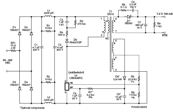
Figure 1 is a circuit diagram of a universal input 7.6 V, 700 mA constant voltage/constant current flyback power supply designed using LinkSwitch-II device LNK606PG, which is suitable for LED driver applications.

LNK606PG (U1) integrates the power switching device, oscillator, CC/CV control engine, and start-up and protection functions into the IC.
Diodes D1 to D4 rectify the AC input. Capacitors C1 and C2 filter the rectified AC. These capacitors, together with inductors L1 and L2, can also attenuate differential mode conducted EMI noise. Resistors R1 and R2 can damp the resonance oscillation generated between these capacitors and the inductor. The combination of the above design and Power Integrations’ transformer E-sheild™ technology allows the power supply to easily meet EN55015 Class B conducted EMI requirements with a margin greater than 10 dB without the need for Y capacitors. The fusible resistor RF1 is used to limit the inrush current generated during startup and acts as a fuse when the component fails due to excessive input current.
This power supply design utilizes U1's integrated constant current characteristics to drive LED loads and can work with maximum output power in constant current mode. IC U1's constant voltage mode can provide output overvoltage protection in the event of any LED open circuit failure.
When working in the constant current phase, U1 adjusts the output current by changing the switching frequency of the MOSFET. As the output voltage increases, U1 will increase its switching frequency. The output voltage is determined by the number of LEDs in the load. The values of resistors R5 and R6 determine the maximum switching frequency and output voltage. The inductance of the transformer ensures that the driver always works at maximum power.
If an output failure occurs, the power supply will operate in constant voltage mode and use the on/off control method to adjust the output voltage. This can provide automatic output fault protection and reduce power consumption in this case. The automatic restart function of IC U1 provides output short circuit protection.
IC U1 is fully self-powered through the BP (bypass) pin and decouples capacitor C4, while also providing high frequency decoupling. When the internal MOSFET turns on, U1 uses the energy stored in C4; when the MOSFET turns off, the internal 6 V regulator draws current from the drain pin. This eliminates the need for external bias windings. Adding an external bias winding will further reduce no-load power consumption.
The rectified and filtered input voltage is applied to one side of the primary winding of T1. The integrated MOSFET in U1 drives the other side of the transformer primary winding. D5, R3, R4 and C3 form an RCD-R clamp circuit to limit the drain voltage spike caused by leakage inductance. IC U1 automatically compensates for tolerance differences in the primary magnetizing inductance. The output power is directly proportional to the set primary inductance, and the output power change can be detected at the FB pin. When the output power changes, the switching frequency will be adjusted to compensate for inductance fluctuations.
Diode D7 (Schottky barrier diode is used to improve efficiency) is used for the secondary output of the rectifier transformer, and C7 filters it. Resistor R8 and capacitor C6 eliminate high-frequency conducted and radiated EMI. When no load is connected, the dummy load resistor R9 acts as a bleeder resistor for C7.
Three, design points
1. The creepage distance between the high-voltage pin and the low-voltage pin on U1 is very large, which can avoid arcing and further improve reliability, which is particularly important under high humidity or high pollution conditions.
2. Capacitor C7 has inefficient series impedance (ESR), which can reduce the output voltage ripple and eliminate the LC post-stage filter.
3. The feedback resistors R5 and R6 should have a tolerance value of 1%, which helps to strictly control the rated output voltage and constant current adjustment threshold at the center position.
4. Using external bias winding can further reduce no-load power consumption. Place the bypass pin capacitor close to U1 on the PCB.
5. Reduce the loop area of the clamp and output diode to reduce EMI.
6. Keep the AC input and the switch node at a certain distance to reduce noise coupling that may bypass input filtering.
7. Make sure that the peak drain voltage of the U1D pin is lower than 650 V, otherwise, it needs to be achieved by reducing the value of R3.
If you want to know more, our website has product specifications for LED driver, you can go to ALLICDATA ELECTRONICS LIMITED to get more information

